Expand menu
Hello, Sign in
My Account
0
Cart
Home
Products
Sensors
Semiconductors
Passive Components
Connectors
Power
Electromechanical
Optoelectronics
Circuit Protection
Integrated Circuits - ICs
Main Products
Manufacturers
Blog
Services
About OMO
About Us
Contact Us
Check Stock
TDA8920CJ/N1,112
P1-P3
P4-P6
P7-P9
P10-P12
P13-P15
P16-P18
P19-P21
P22-P24
P25-P27
P28-P30
P31-P33
P34-P36
P37-P39
xxxxxxxxxxxxxxxxxxxxx xxxxxxxxxxxxxxxxxxxxxxxxxx xxxxxxx x x x xxxxxxxxxxxxxxxxxxxxxxxxxxxxxx xxxxxxxxxxxxxxxxxxx xx xx
xxxxx xxxxxxxxxxxxxxxxxxxxxxxxxxx xxxxxxxxxxxxxxxxxxx xxxxxx xxxxxxxxxxxxxxxxxxxxxxxxxxxxxxxxxxx xxxxxxxxxxxx x x
xxxxxxxxxxxxxxxxxxxxx xxxxxxxxxxxxxxxxxxxxxxxxxxxxxx xxxxx xxxxxxxxxxxxxxxxxxxxxxxxxxxxxxxxxxxxxxxxxxxxxxxxxx xxxxxxxx
xxxxxxxxxxxxxxxxxxxxxxxxx xxxxxxxxxxxxxxxxxxxx xxx
TDA8920C_2
© NXP B.V
. 2009. All rights reserved.
Product data sheet
Rev
. 02 — 11 June 2009
22 of 39
NXP Semiconductors
TD
A8920C
2
×
110 W class-D po
wer amplifier
(1)
The value of C
PRO
T
can be in the range 10 pF to 220 pF (see
Section 8.3.2
)
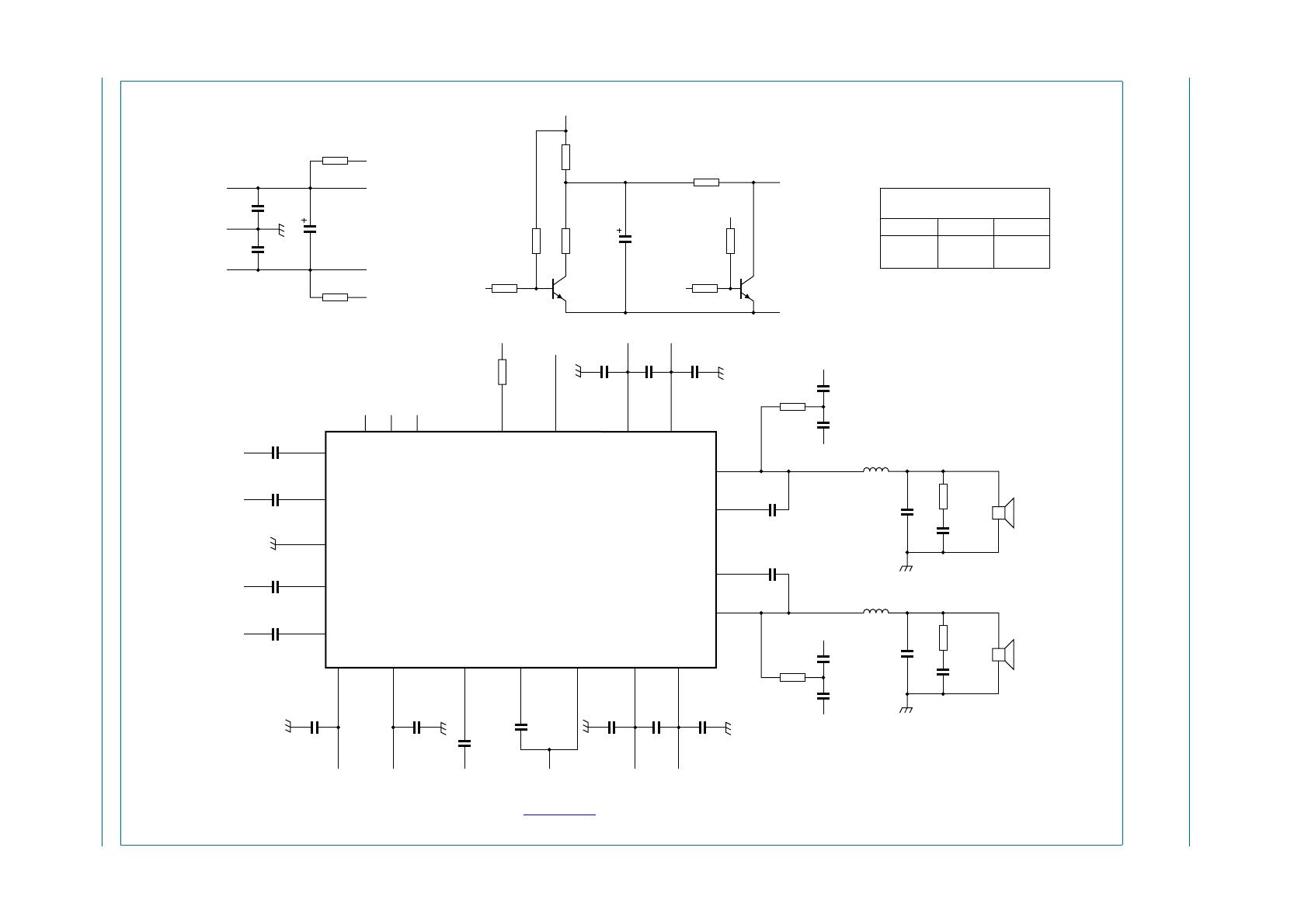
Fig 10.
T
ypical application diagram
010aaa555
C
IN
IN1P
IN1
+
−
+
−
IN2
IN1M
SGND
2
3
19
22
21
20
18
470 nF
470 nF
C
IN
C
IN
IN2P
IN2M
470 nF
470 nF
C
IN
220 nF
VDDA
VSSA
17
7
V
SSP
VDDA
VSSA
PROT
13
14
15
VSSP
VSSP2
OUT2
BOOT2
16
VDDP
VDDP2
VSSD
C
VDDA
220 nF
C
VSSA
100 nF
C
VDDP
15 nF
C
BO
100 nF
C
VSSP
100 nF
C
VP
VSSP
VSSP
VSSP
VDDP
VDDP
VDDP
+
−
+
−
11
VSSP1
8
VDDP1
23
MODE
mode
control
1
OSC
6
4
n.c.
5
n.c.
n.c.
100 nF
C
VDDP
100 nF
C
VSSP
100 nF
C
VP
C
PRO
T
(1)
V
SSA
12
STABI
C
ST
AB
470 nF
R
OSC
30 k
Ω
10
9
OUT1
BOOT1
15 nF
C
BO
L
LC
VSSA
R
VDDA
10
Ω
R
VSSA
10
Ω
C
VP
22
µ
F
C
VDDP
470
µ
F
C
VSSP
470
µ
F
GND
VDDP
VSSP
VDDA
VDDP
VSSP
VSSA
R
SN
10
Ω
R
SN
10
Ω
C
SN
220 pF
C
SN
220 pF
C
SN
220 pF
C
LC
C
LC
C
SN
220 pF
R
ZO
22
Ω
C
ZO
100 nF
R
ZO
22
Ω
C
ZO
100 nF
LOAD
L
LC
C
LC
3
Ω
to 6
Ω
15
µ
H
680 nF
4
Ω
to 8
Ω
22
µ
H
470 nF
SINGLE-ENDED
OUTPUT FILTER VALUES
TDA8920C
L
LC
SGND
mode control
mute/
operating
10
µ
F
5.6 k
Ω
+
5 V
470
Ω
standby/
operating
5.6 k
Ω
T2
HFE > 80
T1
HFE > 80
470 k
Ω
+
5 V
470 k
Ω
10 k
Ω
10 k
Ω
TDA8920C_2
© NXP B.V
. 2009. All rights reserved.
Product data sheet
Rev
. 02 — 11 June 2009
23 of 39
NXP Semiconductors
TD
A8920C
2
×
110 W class-D po
wer amplifier
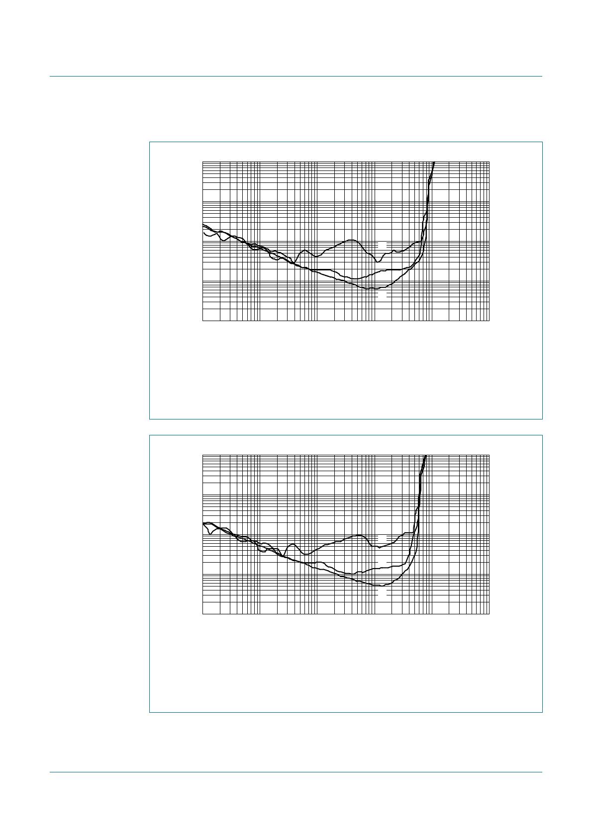
13.8
Curves measured in reference design
V
P
=
±
30 V
, f
osc
= 350 kHz, 2
×
4
Ω
SE configuration.
(1)
f
i
= 6 kHz.
(2)
f
i
= 1 kHz.
(3)
f
i
= 100 Hz.
Fig 11.
THD + N as a function of output power
, SE configuration with 2
×
4
Ω
load
V
P
=
±
30 V
, f
osc
= 350 kHz, 2
×
6
Ω
SE configuration.
(1)
f
i
= 6 kHz.
(2)
f
i
= 1 kHz.
(3)
f
i
= 100 Hz.
Fig 12.
THD + N as a function of output power
, SE configuration with 2
×
6
Ω
load
010aaa532
10
−
1
10
−
2
1
10
THD
(%)
10
−
3
P
o
(W)
10
−
2
10
3
10
2
10
−
1
11
0
(1)
(2)
(3)
010aaa533
10
−
1
10
−
2
1
10
THD
(%)
10
−
3
P
o
(W)
10
−
2
10
3
10
2
10
−
1
11
0
(1)
(2)
(3)
TDA8920C_2
© NXP B.V
. 2009. All rights reserved.
Product data sheet
Rev
. 02 — 11 June 2009
24 of 39
NXP Semiconductors
TD
A8920C
2
×
110 W class-D po
wer amplifier
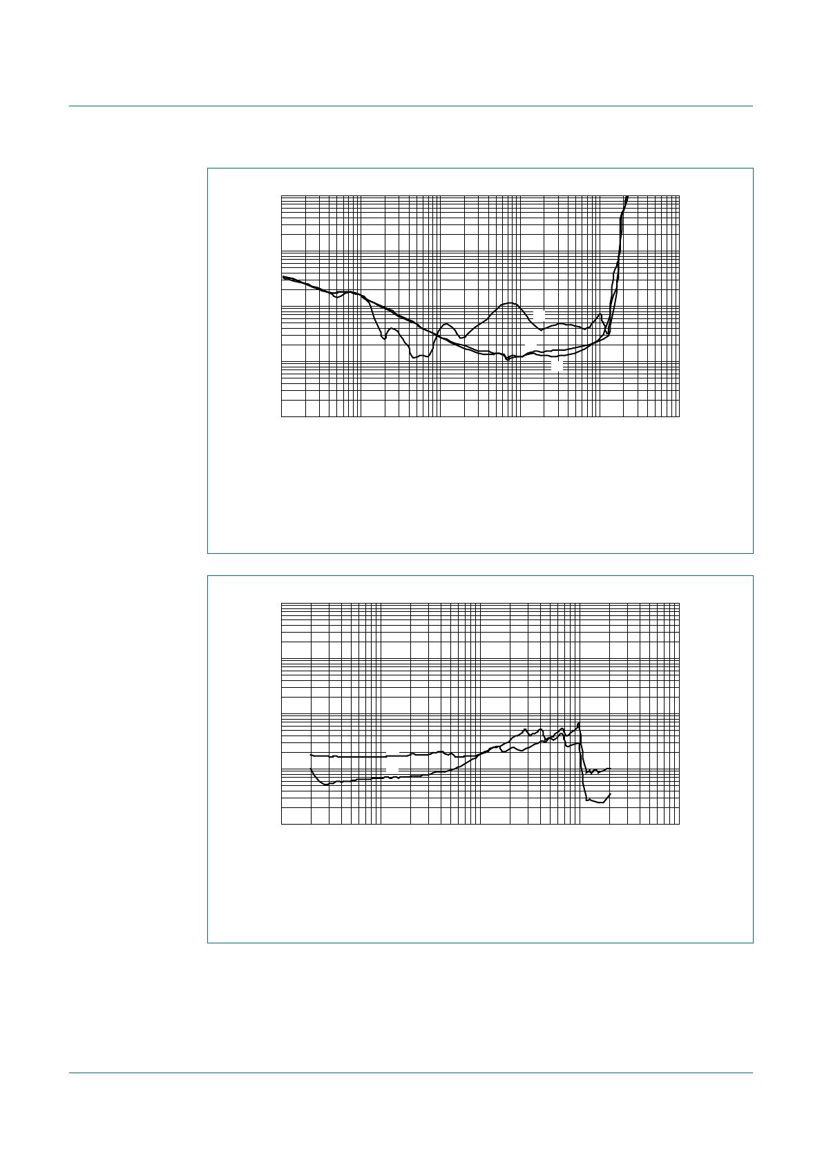
V
P
=
±
30 V
, f
osc
= 350 kHz, 1
×
8
Ω
BTL configuration.
(1)
f
i
= 6 kHz.
(2)
f
i
= 1 kHz.
(3)
f
i
= 100 Hz.
Fig 13.
THD + N as a function of output power
, BTL configuration with 1
×
8
Ω
load
V
P
=
±
30 V
, f
osc
= 350 kHz, 2
×
4
Ω
SE configuration.
(1)
P
o
= 1 W
.
(2)
P
o
= 10 W
.
Fig 14.
THD + N as a function of frequency
, SE configuration with 2
×
4
Ω
load
010aaa534
10
−
1
10
−
2
1
10
THD
(%)
10
−
3
P
o
(W)
10
−
2
10
3
10
2
10
−
1
11
0
(1)
(2)
(3)
010aaa535
10
−
1
10
−
2
1
10
THD
(%)
10
−
3
f
i
(Hz)
10
10
5
10
4
10
2
10
3
(1)
(2)
P1-P3
P4-P6
P7-P9
P10-P12
P13-P15
P16-P18
P19-P21
P22-P24
P25-P27
P28-P30
P31-P33
P34-P36
P37-P39
TDA8920CJ/N1,112
Mfr. #:
Buy TDA8920CJ/N1,112
Manufacturer:
NXP Semiconductors
Description:
Audio Amplifiers Audio Amp Speaker 1CH Mono/2-CH Stereo
Lifecycle:
New from this manufacturer.
Delivery:
DHL
FedEx
Ups
TNT
EMS
Payment:
T/T
Paypal
Visa
MoneyGram
Western
Union
Products related to this Datasheet
TDA8920CTH/N1,118
TDA8920CJ/N1,112