Si3453
Rev. 1.3 13
4.2. Classification
Following a successful PD detection, the classification phase will be automatically initiated in all operational
modes. During this phase, a single measurement will be made at 18 V to determine how much power the PD
device will draw under maximum loads per the IEEE 802.3af and 802.3at standards. The current limit during this
test mode is 60 mA nominal.
The Si3453 supports 1-Event and 2-Event classification. When operating in PoE (<
15.4 W) mode, 1-Event
classification is used. Operation in PoE+ (>15.4 W) mode results in 2-Event classification probes. The 1-Event
classification is compliant to IEEE standard 802.3-2005. 2-Event classification is compliant to draft IEEE P802.3at.
4.3. Port Turn-On and Power FETs
The FET is turned on with a gate drive that results in a very low-noise turn-on waveform with a slew rate of less
than 1 V/µsec (See Figure 5).
The power FET switch on each port has been sized to have a typical ON resistance of approximately 0.3 . The
shunt resistor for current measurement has also been set to 0.1 . Including interconnection and process variation,
the total resistance to VEE for a port that is on is 0.6 (max). This limits the maximum power dissipation per
channel to < 250 mW when the operating current is 600 mA, the maximum current allowed by the IEEE 802.3at
PoE+ standard.
The FET has a programmable operating current limit. Each channel can be set to support output currents of
400 mA or 800 mA minimum.
In addition to the normal current limit, there is a short circuit current shutdown approximately 25% greater than the
nominal current limit. If there is a transient current surge where the current ramps up faster than the programmed
current limit can respond, the gate drive voltage is clamped immediately to V
EE
. The clamp is enabled for at least
10 µs, which allows the normal current circuitry to respond.
Another important protection feature is foldback current limiting. When V
OUT
is near V
EE
, the current limit is at
maximum. As the V
DS
of the driver switch increases (and V
OUT
is closer to ground), the current limit goes to its
lowest level. The amount of the foldback current is scaled proportionally with the programmed current limit.
Figure 5. Turn-On Waveform—Vport Relative to GND
Si3453
14 Rev. 1.3
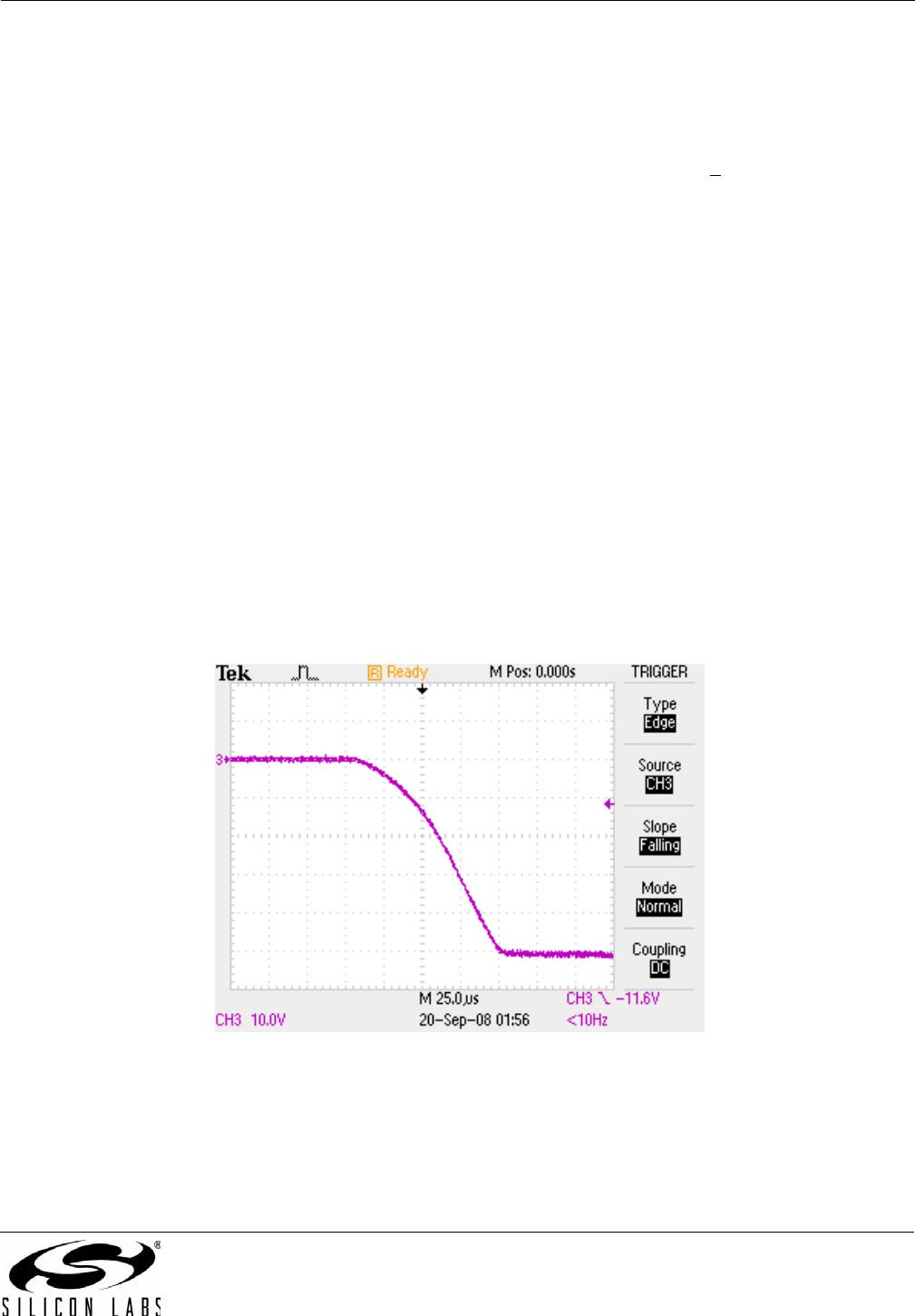
4.4. Disconnect Detection
The port current is continuously monitored by the Si3453. The Si3453 can dynamically change the measurement
scale to achieve accuracy over a wide range of currents.
As defined in the IEEE 802.3 PoE standard, the PSE should disconnect if the port current is less than a nominal
7.5 mA for more than 350 ms.
4.5. Transient Voltage Surge Suppression
The Si3453 features robust on-chip surge protectors on each port; this is an industry first. This unique protection
circuitry acts as an active device that can withstand lightning-induced transients as well as large ESD transient
events. When the port voltage exceeds its protection limit and the current reaches a triggering threshold, current is
shunted from the port to the ground pins.
Internal circuitry is provided to protect the line outputs from externally-coupled fault currents. These are transient
currents of up to 5 A peak.
The operation of the protection circuits depends on the operating mode of the channel switch and the direction of
the fault current. The clamping operation is performed on the detect pin.
The switch itself will also be protected by the current limit. If the transient lasts long enough to heat up the die, then
the temperature sense circuit will shut off the switch, and all the fault current will flow through the clamp diode.
4.6. Temperature Sense
A temperature sense signal is used in conjunction with the current limit status signals from the gate drive blocks.
Any channel that is generating excess heat is assumed to be operating in current limit mode, with both high voltage
drop and high current.
If the port is in PoE mode, an overload will generally not result in thermal shutdown before the 60 ms I
CUT
period. If
the port is in PoE+ mode, an overload may cause the port to shut down prior to the 60 ms I
CUT
period. In either
case, the event is reported as I
CUT
. The faster shutdown in PoE+ mode is consistent with and specifically allowed
by the 802.3at draft and provides much more robust overload protection than is possible with external FETs.
In addition, there is a thermal shutdown if the package temperature exceeds 120 °C. If this threshold is reached, all
output drivers are turned off and detection modes are disabled. This secondary threshold limit guards against the
possibility that the overheating is not caused by a driver operating in current limit.
4.7. Port Measurement and Monitoring
VEE monitoring in conjunction with port current monitoring allows measurement of port power. Port power
monitoring, dynamic power allocation via LLDP*, and port power policing allow efficient power supply sizing.
The Si3453 is factory-calibrated and temperature-compensated for the following measurements:
Port current measurement. These measurements are auto-ranged and scaled to a 16 bit number at 100 µA per
bit. Port current accuracy is ±4% ± 2 mA.
V
EE
is measured with a scale of 64 V. The measurement is reported as a 16-bit number scaled at 1 mV per bit.
V
EE
measurement accuracy is ±4% over the valid V
EE
range.
*Note: LLDP = Link Layer Discovery Protocol. Refer to IEEE 802.3at (draft) and IEEE 802.1AB for more information.
Si3453
Rev. 1.3 15
4.8. SMBus/I
2
C Interface Description
The I
2
C interface is a two-wire, bidirectional serial bus. The I
2
C is compliant with the System Management Bus
Specification (SMBus), version 1.1 and compatible with the I
2
C serial bus. Reads and writes to the interface by the
system controller are byte-oriented with the I
2
C interface autonomously controlling the serial transfer of the data. A
method of extending the clock-low duration is available to accommodate devices with different speed capabilities
on the same bus. The I
2
C provides control of SDA (serial data), SCL (serial clock) generation and synchronization,
arbitration logic, and START/STOP control and generation.
A typical I
2
C transaction consists of a START condition followed by an address byte (Bits7–1: 7-bit slave address;
Bit0: R/W direction bit), one or more bytes of data, and a STOP condition. Each byte that is received (by a master
or slave) must be acknowledged (ACK) with a low SDA during a high SCL (see Figure 6). If the receiving device
does not ACK, the transmitting device will read a NACK (not acknowledge), which is a high SDA during a high
SCL.
The direction bit (R/W) occupies the least-significant bit position of the address byte. The direction bit is set to logic
1 to indicate a “READ” operation and cleared to logic 0 to indicate a “WRITE” operation. All transactions are
initiated by a master, with one or more addressed slave devices as the target. The master generates the START
condition and then transmits the slave address and direction bit. If the transaction is a WRITE operation from the
master to the slave, the master transmits the data one byte at a time, waiting for an ACK from the slave at the end
of each byte.
For READ operations, the slave transmits the data waiting for an ACK from the master at the end of each byte. At
the end of the data transfer, the master generates a STOP condition to terminate the transaction and free the bus.
Figure 6 illustrates a typical SMBus/I
2
C transaction.
Silicon Laboratories recommends the use of bidirectional digital isolators, such as the Si840x, to isolate the I
2
C
communications interface between the Si3453 high-voltage port controllers and the system host controller.
Figure 6. Typical I
2
C Bus Transactions
The Si3453 does not support the alert response address (ARA) protocol. Polling is used to determine which
controller is interrupting in an interrupt-driven system.
0 1 0 A3A2A1A0R/W#
ACK by IC
A7 A6 A5 A4 A 3 A2 A1 A0
ACK by IC
D7 D6 D5 D4 D3 D2 D1 D0
ACK by IC ST OP by MasterST ART
Fixed IC
Address
Pin Set IC
Address
Slave Address Register Address Write Data
010A3A2A1A0R/W#
ACK by IC
A7 A6 A5 A4 A3 A 2 A1 A0
ACK by ICSTART
Fixed IC
Addr ess
Pin Set IC
Addr ess
S lav e Address
Register Address
Setup Register Address
START
0 1 0 A3A2A1A0R/W#
ACK by IC
D7 D6 D5 D4 D3 D2 D1 D0
Not ACK by Master
STOP by Master
Fixed IC
Address
Pin Set IC
Addr ess
Slave Address
Register Data
Transfer Data to Setup Address
Write Sequence
Read Sequence

SI3453B-B02-GM

Mfr. #:
Manufacturer:
Silicon Labs
Description:
Hot Swap Voltage Controllers
Lifecycle:
New from this manufacturer.
Delivery:
DHL FedEx Ups TNT EMS
Payment:
T/T Paypal Visa MoneyGram Western Union