Si3453
4 Rev. 1.3
1. Electrical Specifications
Unless noted otherwise, specifications apply over the operating temperature range with VDD = +3.3 V and
VEE = –48 V relative to GND.
VDD pins should be electrically shorted. AGND pins, DGND, GND12, and GND34 should be electrically shorted
(“GND”). VEE, VEE1, VEE2, VEE3, and VEE4 should be electrically shorted (“VEE”).
VPort for any port is measured from GND to the respective VOUTn.
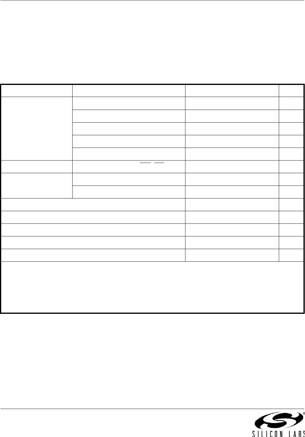
Table 1. Absolute Maximum Ratings
1
Type Description Rating Unit
Supply Voltages
VEE to GND –62 to +0.3 V
VDD to GND –0.3 to +3.6 V
VDD1 to VDD2 –0.3 to +0.3 V
Any VEE to any other VEE –0.3 to +0.3 V
Any GND to any other GND –0.3 to +0.3 V
Voltage on Digital Pins
SDA, SCL, ADn, RST
, INT (GND – 0.3) to (VDD + 0.3) V
Voltage on Analog Pins
VREF, AIN, AOUT, RBIAS, OSC (GND – 0.3) to (VDD + 0.3) V
VOUTn, DETn (VEE – 0.3) to (GND + 0.3) V
DETn Peak Currents During Surge Events
2
±5 A
Maximum Continuous Power Dissipation
3
1.2 W
Maximum Junction Temperature
125 °C
Ambient Storage Temperature
–55 to 150 °C
Lead Temperature (Soldering, 10 seconds Maximum)
260 °C
Notes:
1. Functional operation should be restricted to those conditions specified in Table 2. Functional operation or specification
compliance is not implied at these conditions. Stresses beyond those listed in absolute maximum ratings may cause
permanent damage to the device.
2. See IEEE Std 802.3-2005, clause 33.4, for a description of surge events.
3. If all ports are on with 600 mA load, the power dissipation is <1.2 W. At 85 °C ambient with the expected 32 °C/W
thermal impedance, the junction temperature would be 123.4 °C, which is within the 125 °C maximum rating.
Si3453
Rev. 1.3 5
Table 2. Recommended Operating Conditions
Description Symbol Test Conditions Min Typ Max Unit
Ambient Operating
Temperature
T
A
–40 85 °C
Thermal Impedance* θ
JA
No airflow 32
°C/W
1 m/s airflow 28
Power Supply Voltages
V
EE
Supply Voltage V
EE
For IEEE 802.3af (15.4 W) apps. –57 –48 –45 V
For IEEE 802.3at (30 W) apps. –57 –54 –51 V
V
DD
Supply Voltage V
DD
3.0 3.3 3.6 V
Power Supply Currents
V
EE
Supply Current I
EE
All ports on, excluding load current. 3.7 6.0
mA
All ports in shutdown mode 1 2
V
DD
Supply Current I
DD
—814mA
*Note: Modeled with six parts evenly spaced on a 30 x 120 mm2, four-layer board with 25 thermal vias to a Vneg plane on the
back.
Table 3. UVLO, and Reset Specifications
Description Symbol Test Conditions Min Typ Max Unit
V
DD
Reset Threshold V
RST
—1.75 V
V
DD
Power-On Ramp
*
Ramp from 0 V to 3.0 V 1 ms
RST
Input High Voltage 0.7 x V
DD
—— V
RST
Input Low Voltage 0.8 V
RST Input Leakage RST
=0V 40 μA
Reset Time Delay T
RSTDLY
Time between end of reset and
beginning of normal operation
——100ms
Reset Assertion Time T
RST
RST low time to generate system
reset
15 μs
V
EE
Monitor Accuracy V
EEMON
Measured V
EE
relative to actual
V
EE
for V
EE
(–44 to –57 V)
–4 4 %
V
EE
UVLO Threshold V
UVLO
Point at which VEE UVLO is
declared.
VEE going negative
VEE going positive
–38
–36
–33
–31
V
*Note: If VDD ramp time is slower than 1 ms, hold the reset pins low until VDD is above 3.0 V to insure proper reset
operation.
Si3453
6 Rev. 1.3
Table 4. Detection Specifications
Description Symbol Test Conditions Min Typ Max Unit
Detection Current Limit I
LIM_DET
Measured with DETn
shorted to GND
—3 5mA
Detection Voltage,
when R
DET
=25k
V
DET1
V
DET2
V
DET3
–10.0
–4.0
–8.0
–4.0
–2.8
–2.8
V
Detection Slew Rate 0.1 V/μs
Detection Probe Duration T
PROBE
10 30 ms
Detection Probe Cycle Time T
DET
——500ms
Minimum Valid Signature Resistance R
DET_MIN
15 19 k
Maximum Valid Signature Resistance R
DET_MAX
26.5 33 k
Resistance at which Open Circuit is
Declared
R
OPEN
100 400 k
Resistance at which Short Circuit is
Declared
R
SHORT
150 400 W
Valid Detect Capacitance C
DET_VALID
——150nF
Invalid Detect Capacitance C
DET_INVALD
10 μF
Table 5. Classification Specifications
Description Symbol Test Conditions Min Typ Max Unit
Class Event Voltage V
CLASS
0mA < I
Port
< 45 mA –20.5 –15.5 V
Mark Event Voltage V
MARK
0mA < I
Port
< 5 mA –7 –10 V
Classification Current
Limit
I
LIM_CLASS
Measured with DETn shorted to
GND
51 100 mA
Classification Current
Regions
Class 0
Class 1
Class 2
Class 3
Class 4
Overcurrent
0
8
16
25
35
51
5
13
21
31
45
mA
Classification Delay T
CLASS_DLY
Time from end of valid detect cycle
to classification begin
—5—ms
Classification Event
Time
T
CLE
Width of valid V
CLASS
probe for 1-
Event or 2-Event classification
10 30 ms
Mark Event Time T
ME
Width of mark between classification
events
—8—ms

SI3453B-B02-GM

Mfr. #:
Manufacturer:
Silicon Labs
Description:
Hot Swap Voltage Controllers
Lifecycle:
New from this manufacturer.
Delivery:
DHL FedEx Ups TNT EMS
Payment:
T/T Paypal Visa MoneyGram Western Union