Si3453
28 Rev. 1.3
9. Pin Descriptions
Table 25. Si3453 Pin Descriptions
Pin # Name Type Description
1 VEE1 Supply Driver 1 VEE supply. Short to VEE, VEE2/3/4.
2 VEE Supply Global PoE (–48 V nom.) or PoE+ (–54 V nom.) supply. Short to VEE1/2/
3/4.
3 VREF Analog input 1.1 V nom. voltage reference from reference generator (for example,
TLV431 or power management unit).
4 AIN Analog input Measurement data converter input. Short to AOUT.
5 AOUT Analog output Measurement multiplexer subsystem output. Short to AIN.
6 AGND Ground Analog ground reference. Short to AGND pin 8, GND12/34, DGND.
7 RBIAS Analog input External 44.2 k (±1%) resistor to ground sets internal bias currents.
8 AGND Ground Analog ground reference. Short to AGND pin 6, GND12/34, DGND.
9 NC No connect Do not connect (float).
10 VEE4 Supply Driver 4 VEE supply. Short to VEE, VEE1/2/3.
11 NC No connect Do not connect (float).
12 VOUT4 Analog I/O Port 4 power FET switch output. When on, provides a low impedance
path to VEE4.
VEE
VEE1
AIN
RBIAS
VREF
AGND
AOUT
1
2
3
4
5
6
7
AGND
8
DGND
VDD
AD1
AD3
AD0
AD2
AD2
30
29
28
27
26
25
24
VOUT4
NC
SDA
NC
DET4
SCL
GND34
11
12
13
14
15
16
17
DET3
18
VDD
19
39
38
37
36
35
34
33
VOUT1
INT
DET1
AD0
RST
GND12
AD1
DET2
VEE4
10
NC
9
VEE3
22
RST
23
AD3
21
VOUT3
20
32
VOUT2
31
VEE2
Si3453
(Top View)
40
Si3453
Rev. 1.3 29
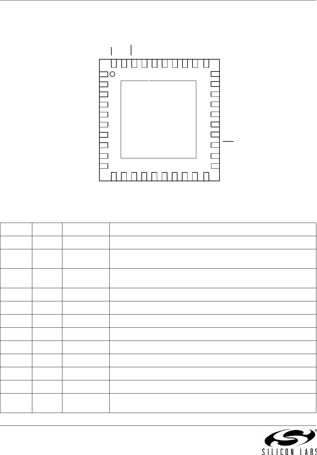
13 DET4 Analog I/O Connection for port 4 detection, classification, and transient surge protec-
tion. This pin is tied to VOUT4.
14 SDA Digital I/O I
2
C data pin
15 GND34 Ground Ground supply for protection clamps. Short to AGND, GND12, DGND.
16 SCL Digital I/O I
2
C clock pin
17 NC No connect Do not connect (float).
18 DET3 Analog I/O Connection for port 3 detection and classification. See DET4 for detailed
description.
19 VDD Supply +3.3 V (±10%) isolated supply. Short to VDD pin 30.
20 VOUT3 Analog I/O Port 3 power FET switch output. When on, provides a low impedance
path to VEE3.
21 AD3 Digital I/O Chip address bit 3 pin, read after reset. Address set with defined resistor
dividers. Pin also used for internal communications. Short to AD3 pin 24.
22 VEE3 Supply Driver 3 VEE supply. Short to VEE, VEE1/2/4.
23 RST Digital input Active low digital reset. Short to RST
pin 38.
24 AD3 Digital I/O Chip address bit 3 pin, read after reset. Address set with a 10 kpull-up
or pull-down resistor. Also used for internal communications. Short to
AD3 pin 21.
25 AD2 Digital I/O Chip address bit 2 pin, read after reset. Address set with a 10 kpull-up
or pull-down resistor. Also used for internal communications. Short to
AD2 pin 26.
26 AD2 Digital I/O Chip address bit 2 pin, read after reset. Address set with a 10 kpull-up
or pull-down resistor. Also used for internal communications. Short to
AD2 pin 25.
27 AD1 Digital I/O Chip address bit 1 pin, read after reset. Address set with a 10 kpull-up
or pull-down resistor. Also used for internal communications. Short to
AD1 pin 36.
28 AD0 Digital I/O Chip address bit 0 pin, read after reset. Address set with a 10 kpull-up
or pull-down resistor. Also used for internal communications. Short to
AD0 pin 34.
29 DGND Ground Digital ground reference. Short to AGND, GND12/34
30 VDD Supply +3.3 V isolated supply. Short to VDD pin 19.
31 VEE2 Supply Driver 2 VEE supply. Short to VEE, VEE1/3/4.
32 VOUT2 Analog I/O Port 2 power FET switch output. When on, provides a low impedance
path to VEE2.
Table 25. Si3453 Pin Descriptions (Continued)
Pin # Name Type Description
Si3453
30 Rev. 1.3
33 DET2 Analog I/O Connection for port 2 detection and classification. See DET4 for detailed
description.
34 AD0 Digital I/O Chip address bit 0 pin. See description for- and short to AD0 pin 28.
35 GND12 Ground Ground supply for protection clamps. Short to AGND, GND34, DGND.
36 AD1 Digital I/O Chip address bit 1 pin. See description for- and short to AD1 pin 27.
37 DET1 Analog I/O Connection for port 1 detection and classification. See DET4 for detailed
description.
38 RST Digital input Active low digital reset. Short to RST
pin 23.
39 VOUT1 Analog I/O Port 1 power FET switch output. When on, provides a low impedance
path to VEE1.
40 INT Digital output Active low interrupt output pin.
ePAD Vee Supply Connect the thermal pad to a plane which connects to Vee. For best
results, use a 5 x 5 or larger via array for best thermal conductivity with 1
square inch or larger of plane area per device.
Table 25. Si3453 Pin Descriptions (Continued)
Pin # Name Type Description

SI3453B-B02-GM

Mfr. #:
Manufacturer:
Silicon Labs
Description:
Hot Swap Voltage Controllers
Lifecycle:
New from this manufacturer.
Delivery:
DHL FedEx Ups TNT EMS
Payment:
T/T Paypal Visa MoneyGram Western Union