Si3453
34 Rev. 1.3
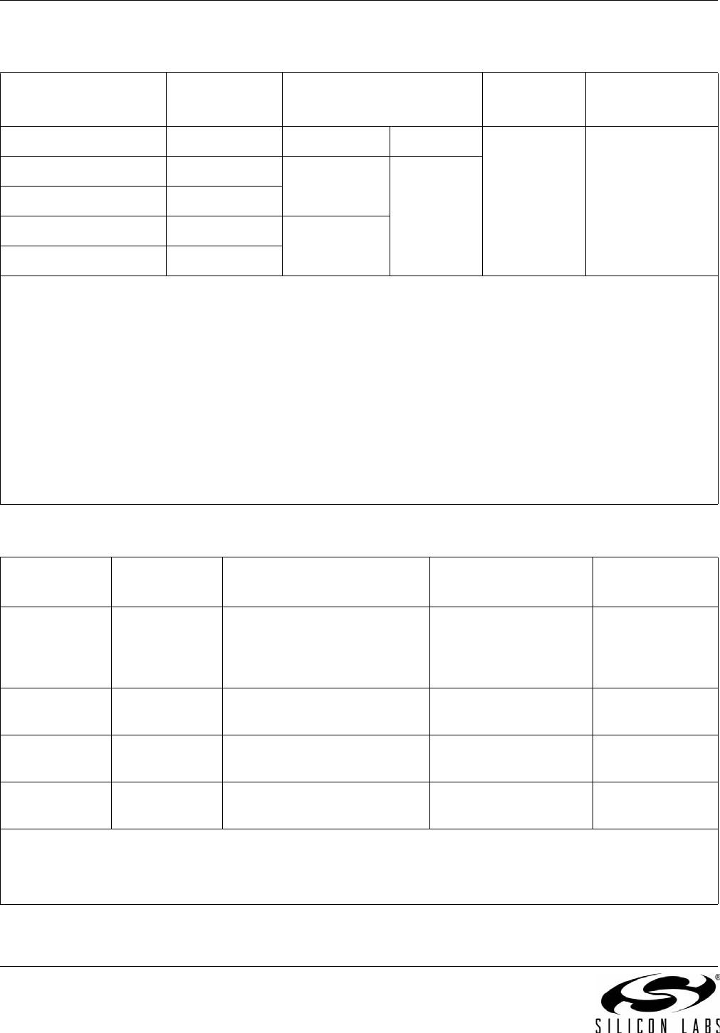
12. Ordering Guide
12.1. Evaluation Kits and Reference Designs
Ordering Part Number
1
Detect
Timing
2
Powerup Mode
2,3,4,5
Firmware
Revision
Package
6
Temp. Range
Si3453-B02-GM Alt A PoE
7
Shutdown 0.2.81 –40 to 85 °C
ambient
Si3453A-B02-GM Alt A PoE (15.4 W) Auto
Si3453B-B02-GM Alt B
Si3453C-B02-GM Alt A PoE+ (30 W)
Si3453D-B02-GM Alt B
Notes:
1.
Add “R” to the end of the ordering part number to denote tape-and-reel option. E.g., Si3452-B02-GMR.
2. For alternative A, power is applied to wire pairs 1,2 and 3,6. For alternative B, power is applied to wire pairs 4,5 and 7,8
(the spare pairs in the case of 10/100 Ethernet). Conventionally, alternative B is used for midspan power injectors. For
alternative B, detection is done with over 2 seconds between detection pulses so as to avoid interfering with end-point
equipment trying to provide power using alternative A.
3. Devices powering up into shutdown mode are intended for use with a system host that provides run-time configuration
or power-management.
4. The maximum PoE or PoE+ power applies to all ports on Auto mode devices.
5. Detect Timing and Powerup Modes (PoE vs. PoE+, Shutdown vs. Auto) are pre-configured in firmware but can be
reconfigured at any time via a host connection.
6. All devices are packaged in RoHS-compliant, 40-pin, 6x6 mm QFN.
7. The Si3453-B02-GM is PoE+ capable. The part defaults to PoE mode at powerup but can be reconfigured to PoE+ via
register settings.
Part Number Populated
Device
Description Related Ethernet
Chipset
Type
Si3452MS8-KIT Si3453-B02-GM PoE+ 8-port Midspan PSE
evaluation kit. Includes PC-
control interface, PD loads, and
cables.
None Evaluation Kit
Si3452V1-RD* Si3453-B02-GM PoE/PoE+ 24-port daughter-
card
Vitesse E-StaX
(VSC7407)
Reference Design
Si3452V2-RD* Si3453-B02-GM PoE+ 8-port Gb-Ethernet
switch
Vitesse SparX-G8e
(VSC7398)
Reference Design
Si3452M1-RD* Si3453-B02-GM PoE/PoE+ 24-port daughter-
card
Marvell Prestera-DX,
xCAT
Reference Design
*Note: Due to unique high-voltage and high-power design considerations, Silicon Laboratories recommends that the
reference designs be followed very closely for both bill of materials and layout. Please visit the Silicon Labs technical
support web page at www.silabs.com/support/pages/contacttechnicalsupport.aspx and register to request support for
your design, particularly if you are not closely following the recommended reference design.