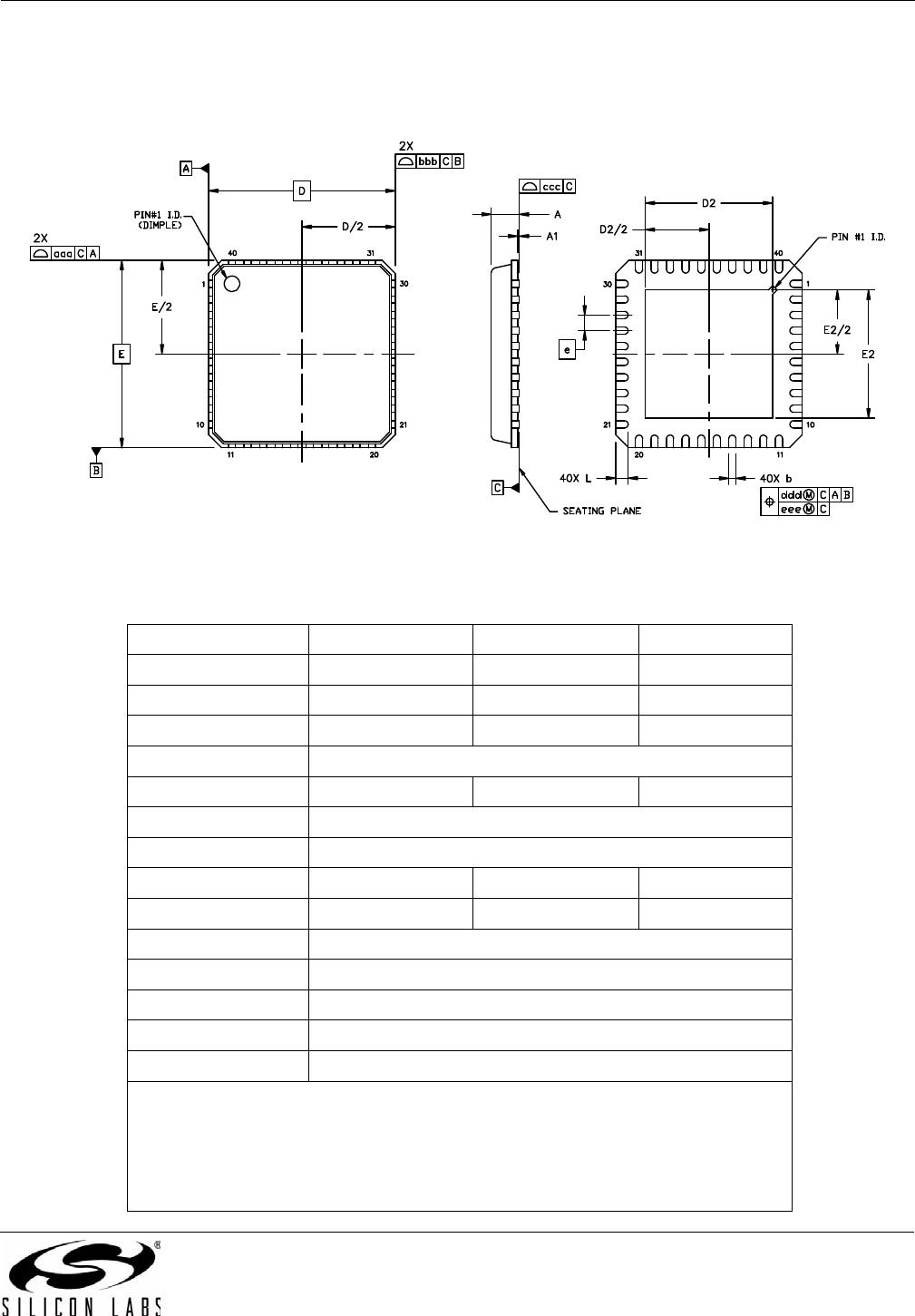
Si3453
Rev. 1.3 33
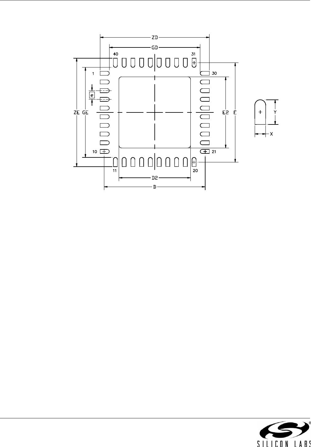
Table 27. PCB Land Pattern Dimensions
Dimension Min Max
e 0.50 BSC
E5.42 REF
D5.42 REF
E2 4.00 4.20
D2 4.00 4.20
GE 4.53 —
GD 4.53 —
X — 0.28
Y0.89 REF
ZE — 6.31
ZD — 6.31
Notes:
General
1.
All dimensions shown are in millimeters (mm) unless otherwise noted.
2. Dimensioning and Tolerancing is per the ANSI Y14.5M-1994 specification.
3. This Land Pattern Design is based on IPC-SM-782 guidelines.
4. All dimensions shown are at Maximum Material Condition (MMC). Least Material
Condition (LMC) is calculated based on a Fabrication Allowance of 0.05 mm.
Solder Mask Design
5. All metal pads are to be non-solder mask defined (NSMD). Clearance between the
solder mask and the metal pad is to be 60 µm minimum, all the way around the pad.
Stencil Design
6. A stainless steel, laser-cut and electro-polished stencil with trapezoidal walls should
be used to assure good solder paste release.
7. The stencil thickness should be 0.125 mm (5 mils).
8. The ratio of stencil aperture to land pad size should be 1:1 for the perimeter pads.
9. A 4x4 array of 0.80 mm square openings on 1.05 mm pitch should be used for the
center Vee pad.
Card Assembly
10. A No-Clean, Type-3 solder paste is recommended.
11. The recommended card reflow profile is per the JEDEC/IPC J-STD-020
specification for Small Body Components.