Si3453
Rev. 1.3 7
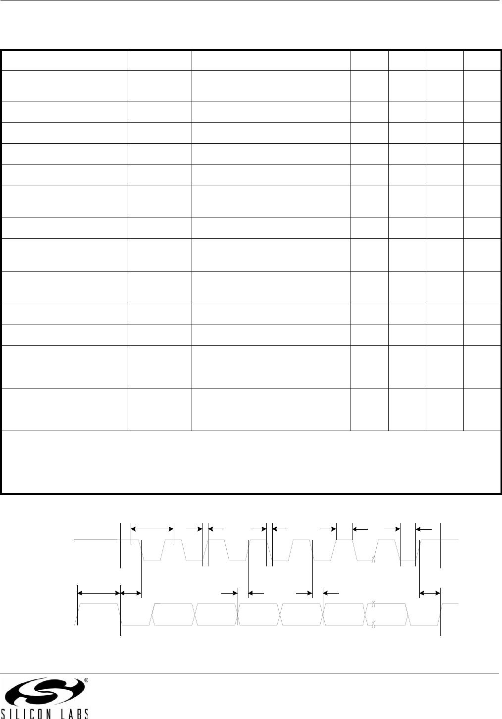
Table 6. VOUT Drive and Power-on Specifications
Description Symbol Test Conditions Min Typ Max Unit
Max Output Resistance
(Port On)
R
ON
I
Port
720 mA 0.3 0.6
Current Limit I
LIM
1x mode, V
port
=V
EE
+ 1 V 400 425 450 mA
Change in Current Limit I
LIM
1x mode, V
port
=V
EE
+ 1V to30V
1
–2 2 %
Current Limit I
LIM
2x mode, V
port
=V
EE
+ 1 V 800 860 920 mA
Change in Current Limit I
LIM
2x mode, V
port
=V
EE
+ 1V to40V
2
–2 2 %
Current Limit I
LIM
1x mode or 2x mode, V
port
=–10V 60 mA
Overload Current
Threshold
I
CUT
Class 0
Class 1 (class policing enabled)
3
Class 2 (class policing enabled)
3
Class 3
Class 4
4
350
91
160
350
600
mA
Over Current Time
Limit
5
T
OVLD
Load current I
CUT
or I
LIM
50 75 ms
VOUTn Turn-on Slew T
RISE
10% to 90% 15 70 µs
Power Turn On Timing T
PON
Time from end of valid detect to
power on
——400ms
VOUTn Leakage Cur-
rent
I
OUT_LEAK
Port in shutdown 10 µA
Notes:
1. T
J
>25 °C, –35 V over the full temperature range.
2. 1x mode current limit is enforced during the 60 ms T
START
time.
3. In auto mode, class policing is automatically enabled. In manual mode, I
CUT
must be programmed manually.
See "5.4. Port Configuration (Registers 0x0A–0x11)" on page 18 for more information.
4. 600 mA is consistent with the IEEE 802.3at draft standard. I
CUT
is user-programmable in 3.2 mA increments to over
800 mA for non-standard applications.
5. For 2x mode and extreme overload or short-circuit events, T
OVLD
will dynamically decrease to prevent excessive FET
heating. This is consistent with the 802.3at draft.
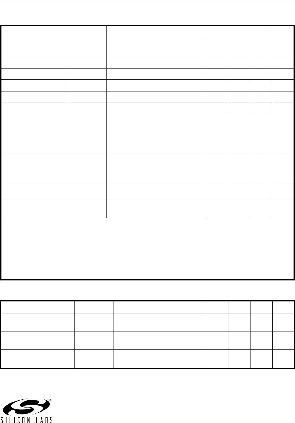
Table 7. DC Disconnect Specifications
Description Symbol Test Conditions Min Typ Max Unit
Load Current to Prevent
Disconnect
I
ON
10 mA
Load Current to
Guarantee Disconnect
I
OFF
dc disconnect 5 mA
Disconnect Delay
T
DCDV_DLY
Time from I
OFF
load current to port
turn off
300 400 ms
Si3453
8 Rev. 1.3
Table 8. Port Measurement and Monitoring Specifications
Description Symbol Test Conditions Min Typ Max Unit
Port Current Measurement
Offset
I
OFFSET
20 mA I
PORT
I
CUT
. For final
I
PORT
reading, add offset to% of
reading tolerance.
–5 5 mA
Port Current Measurement
Tolerance
%
TOL
–4 4 %
Table 9. SMBus (I
2
C) Electrical Specifications
VDD = 3.0 to 3.6 V
Description Symbol Test Conditions Min Typ Max Unit
Input Low Voltage
V
IL
SCL, SDA pins 0.8* V
Input High Voltage
V
IH
SCL, SDA pins 2.2 V
Output Low Voltage
V
OL
SCL, SDA pins,
driving 8.5 mA
——0.6V
Input Leakage Current
I
L
SCL, SDA pins 40 µA
*Note: 0.85 V for T
j
>–10 °C. This ensures compatibility with Si840x isolators with 3 k pull up. For isolator compatibility over
the full temperature range, use Si860x isolators.
Table 10. Address Pin Electrical Specifications*
VDD = 3.0 to 3.6 V
Description Symbol Test Conditions Min Typ Max Unit
Input Low Voltage V
IL
AD0, AD1, AD2, AD3 pins 0.8 V
Input High Voltage V
IH
AD0, AD1, AD2, AD3 pins 0.7 x V
DD
——V
Input Leakage Current I
H
, I
L
AD0, AD1, AD2, AD3 pins –10 10 µA
*Note: At power-up, these pins are logic inputs. A 10 k pull up or pull down resistor is used for address selection. After
address recognition, the pins are used for internal communications.
Si3453
Rev. 1.3 9
Figure 1. I
2
C Timing Diagram
Table 11. SMBus (I
2
C) Timing Specifications (see Figure 1)
VDD = 3.0 to 3.6 V
Description Symbol Test Conditions Min Typ Max Unit
Serial Bus Clock Fre-
quency
f
SCL
0—400kHz
SCL High Time
t
SKH
600 ns
SCL Low Time
t
SKL
1.3 μs
SCL, SDA Rise Time
t
R_SCL
20 300 ns
SCL, SDA Fall Time
t
F_SCL
20 150 ns
Bus Free Time
t
BUF
Between START and STOP
conditions.
1.3 μs
Start Hold Time
t
STH
Between START and first low SCL. 600 ns
Start Setup Time
t
STS
Between SCL high and START
condition.
600 ns
Stop Setup Time
t
SPS
Between SCL high and STOP
condition.
600 ns
Data Hold Time
t
DH
200 ns
Data Setup Time
t
DS
200 ns
Time from Hardware or
Software Reset until Start
of I
2
C Traffic
t
RESET
Reset to start condition 100 ms
Delay from Event to INT
Pin Low or from Clear-On-
Read to INT Pin High
t
INT
—— 5ms
Notes:
1. Not production tested (guaranteed by design).
2. All timing references measured at V
IL
and V
IH
.
3. The Si3453 will stretch (pull down on) SCK during the ACK time period if required. The maximum SCL stretching is
10 µsec; so, SCL only needs to be bidirectional for I
2
C bus speeds over 50 kHz.
SCL
D7
fSC L
tR_SCL tF_SCL tSK H
SDA
tSKL
tSTH tSPS
D6 D5 D4 D3 D0
tDS tDH
Start Bit Stop Bit
tBUF

SI3453B-B02-GM

Mfr. #:
Manufacturer:
Silicon Labs
Description:
Hot Swap Voltage Controllers
Lifecycle:
New from this manufacturer.
Delivery:
DHL FedEx Ups TNT EMS
Payment:
T/T Paypal Visa MoneyGram Western Union