Variant
Member
Code
M10K MLAB
Total RAM Bit
(Kb)Block RAM Bit (Kb) Block RAM Bit (Kb)
Cyclone V GT D5 446 4,460 679 424 4,884
D7 686 6,860 1338 836 7,696
D9 1,220 12,200 2748 1,717 13,917
Cyclone V SE A2 140 1,400 221 138 1,538
A4 270 2,700 370 231 2,460
A5 397 3,970 768 480 4,450
A6 553 5,530 994 621 6,151
Cyclone V SX C2 140 1,400 221 138 1,538
C4 270 2,700 370 231 2,460
C5 397 3,970 768 480 4,450
C6 553 5,530 994 621 6,151
Cyclone V ST D5 397 3,970 768 480 4,450
D6 553 5,530 994 621 6,151
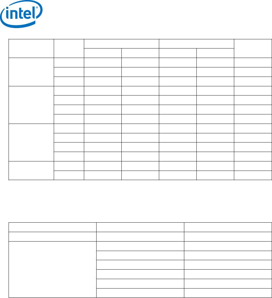
Embedded Memory Configurations
Table 19. Supported Embedded Memory Block Configurations for Cyclone V Devices
This table lists the maximum configurations supported for the embedded memory blocks. The information is
applicable only to the single-port RAM and ROM modes.
Memory Block
Depth (bits) Programmable Width
MLAB 32 x16, x18, or x20
M10K 256 x40 or x32
512 x20 or x16
1K x10 or x8
2K x5 or x4
4K x2
8K x1
Clock Networks and PLL Clock Sources
550 MHz Cyclone V devices have 16 global clock networks capable of up to operation.
The clock network architecture is based on Intel's global, quadrant, and peripheral
clock structure. This clock structure is supported by dedicated clock input pins and
fractional PLLs.
Note: To reduce power consumption, the Intel Quartus Prime software identifies all unused
sections of the clock network and powers them down.
Cyclone V Device Overview
CV-51001 | 2018.05.07
Cyclone V Device Overview
22
PLL Features
The PLLs in the Cyclone V devices support the following features:
Frequency synthesis
On-chip clock deskew
Jitter attenuation
Programmable output clock duty cycles
PLL cascading
Reference clock switchover
Programmable bandwidth
User-mode reconfiguration of PLLs
Low power mode for each fractional PLL
Dynamic phase shift
Direct, source synchronous, zero delay buffer, external feedback, and LVDS
compensation modes
Fractional PLL
In addition to integer PLLs, the Cyclone V devices use a fractional PLL architecture.
The devices have up to eight PLLs, each with nine output counters. You can use the
output counters to reduce PLL usage in two ways:
Reduce the number of oscillators that are required on your board by using
fractional PLLs
Reduce the number of clock pins that are used in the device by synthesizing
multiple clock frequencies from a single reference clock source
If you use the fractional PLL mode, you can use the PLLs for precision fractional-N
frequency synthesis—removing the need for off-chip reference clock sources in your
design.
The transceiver fractional PLLs that are not used by the transceiver I/Os can be used
as general purpose fractional PLLs by the FPGA fabric.
FPGA General Purpose I/O
Cyclone V devices offer highly configurable GPIOs. The following list describes the
features of the GPIOs:
Programmable bus hold and weak pull-up
LVDS output buffer with programmable differential output voltage (V
OD
) and
programmable pre-emphasis
On-chip parallel termination (R
T
OCT) for all I/O banks with OCT calibration to
limit the termination impedance variation
On-chip dynamic termination that has the ability to swap between series and
parallel termination, depending on whether there is read or write on a common
bus for signal integrity
Easy timing closure support using the hard read FIFO in the input register path,
and delay-locked loop (DLL) delay chain with fine and coarse architecture
Cyclone V Device Overview
CV-51001 | 2018.05.07
Cyclone V Device Overview
23
PCIe Gen1 and Gen2 Hard IP
Cyclone V GX, GT, SX, and ST devices contain PCIe hard IP that is designed for
performance and ease-of-use. The PCIe hard IP consists of the MAC, data link, and
transaction layers.
The PCIe hard IP supports PCIe Gen2 and Gen1 end point and root port for up to x4
lane configuration. The PCIe Gen2 x4 support is PCIe-compatible.
The PCIe endpoint support includes multifunction support for up to eight functions, as
shown in the following figure. The integrated multifunction support reduces the FPGA
logic requirements by up to 20,000 LEs for PCIe designs that require multiple
peripherals.
Figure 9. PCIe Multifunction for Cyclone V Devices
PCIe Link
External System
FPGA Device
Host CPU
Memory
Controller
Root
Complex
Local
Peripheral 1
Local
Peripheral 2
PCIe RP
PCIe EP
CAN
GbE
ATA
Bridge
to PCIe
SPI
GPIO
I
2
C
USB
The Cyclone V PCIe hard IP operates independently from the core logic. This
independent operation allows the PCIe link to wake up and complete link training in
less than 100 ms while the Cyclone V device completes loading the programming file
for the rest of the device.
In addition, the PCIe hard IP in the Cyclone V device provides improved end-to-end
datapath protection using ECC.
External Memory Interface
This section provides an overview of the external memory interface in Cyclone V
devices.
Hard and Soft Memory Controllers
Cyclone V devices support up to two hard memory controllers for DDR3, DDR2, and
LPDDR2 SDRAM devices. Each controller supports 8 to 32 bit components of up to
4 gigabits (Gb) in density with two chip selects and optional ECC. For the Cyclone V
SoC devices, an additional hard memory controller in the HPS supports DDR3, DDR2,
and LPDDR2 SDRAM devices.
All Cyclone V devices support soft memory controllers for DDR3, DDR2, and LPDDR2
SDRAM devices for maximum flexibility.
Cyclone V Device Overview
CV-51001 | 2018.05.07
Cyclone V Device Overview
24

5CGXFC7C6U19C7N

Mfr. #:
Manufacturer:
Intel / Altera
Description:
FPGA - Field Programmable Gate Array FPGA - Cyclone V GX 5648 LABs 224 IOs
Lifecycle:
New from this manufacturer.
Delivery:
DHL FedEx Ups TNT EMS
Payment:
T/T Paypal Visa MoneyGram Western Union