REV. 0
AD7708/AD7718
–15–
ADC CIRCUIT INFORMATION
The AD7708/AD7718 incorporates a 10-channel multiplexer
with a sigma-delta ADC, on-chip programmable gain amplifier
and digital filtering intended for the measurement of wide
dynamic range, low frequency signals such as those in weigh-scale,
strain-gauge, pressure transducer, or temperature measurement
applications. The AD7708 offers 16-bit resolution while the
AD7718 offers 24-bit resolution. The AD7718 is a pin-for-pin
compatible version of the AD7708. The AD7718 offers a direct
upgradable path from a 16-bit to a 24-bit system without requiring
any hardware changes and only minimal software changes.
These parts can be configured as four/five fully-differential
input channels or as eight/ten pseudo-differential input chan-
nels referenced to AINCOM. The channel is buffered and can
be programmed for one of eight input ranges from ±20 mV to
±2.56 V. Buffering the input channel means that the part can
handle significant source impedances on the analog input and
that R, C filtering (for noise rejection or RFI reduction) can be
placed on the analog inputs if required. These input channels
are intended to convert signals directly from sensors without the
need for external signal conditioning.
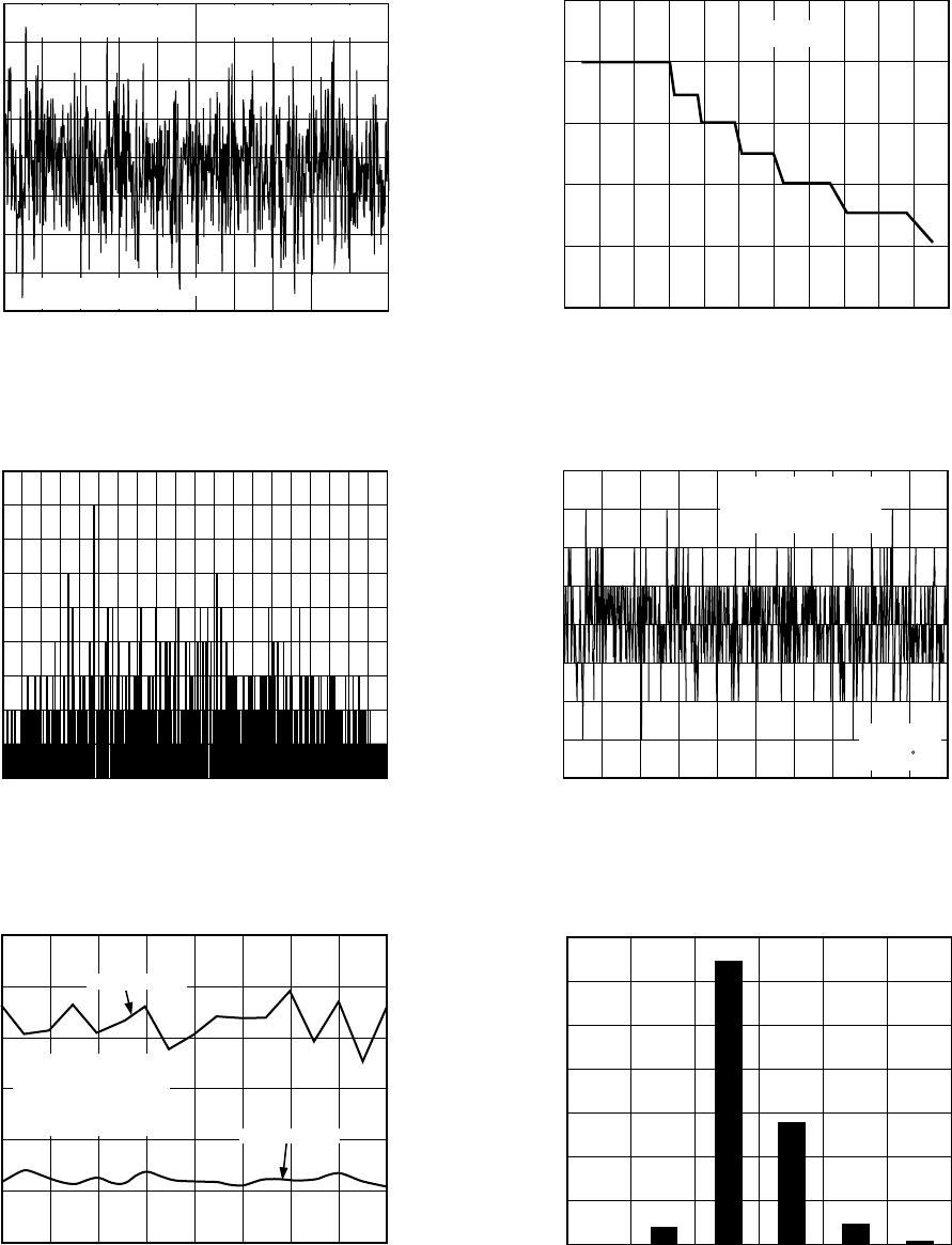
The ADC employs a sigma-delta conversion technique to realize
up to 24 bits of no missing codes performance. The sigma-delta
modulator converts the sampled input signal into a digital pulse
train whose duty cycle contains the digital information. A Sinc
3
programmable low-pass filter is then employed to decimate the
modulator output data stream to give a valid data conversion result
at programmable output rates. The signal chain has two modes
of operation, CHOP enabled and CHOP disabled. The CHOP bit
in the mode register enables and disables the chopping scheme.
Signal Chain Overview (CHOP Enabled, CHOP = 0)
With CHOP = 0, chopping is enabled, this is the default and gives
optimum performance in terms of drift performance. With chopping
enabled, the available output rates vary from 5.35 Hz (186.77 ms)
to 105.03 Hz (9.52 ms). A block diagram of the ADC input
channel with chop enabled is shown in Figure 4.
The sampling frequency of the modulator loop is many times
higher than the bandwidth of the input signal. The integrator in
the modulator shapes the quantization noise (which results from
the analog-to-digital conversion) so that the noise is pushed
toward one-half of the modulator frequency. The output of the
sigma-delta modulator feeds directly into the digital filter. The
digital filter then band-limits the response to a frequency signifi-
cantly lower than one-half of the modulator frequency. In this
manner, the 1-bit output of the comparator is translated into a
band limited, low noise output from the AD7708/AD7718 ADC.
The AD7708/AD7718 filter is a low-pass, Sinc
3
or (sinx/x)
3
filter whose primary function is to remove the quantization noise
introduced at the modulator. The cutoff frequency and deci-
mated output data rate of the filter are programmable via the SF
word loaded to the filter register. The complete signal chain is
chopped resulting in excellent dc offset and offset drift specifica-
tions and is extremely beneficial in applications where drift, noise
rejection, and optimum EMI rejection are important factors.
With chopping, the ADC repeatedly reverses its inputs. The
decimated digital output words from the Sinc
3
filters, therefore,
have a positive offset and negative offset term included. As a
result, a final summing stage is included so that each output
word from the filter is summed and averaged with the previous
filter output to produce a new valid output result to be written
to the ADC data register. The programming of the Sinc
3
deci-
mation factor is restricted to an 8-bit register SF, the actual
decimation factor is the register value times 8. The decimated
output rate from the Sinc
3
filter (and the ADC conversion rate)
will therefore be
f
SF
f
ADC MOD
=×
×
×
1
3
1
8
where
f
ADC
in the ADC conversion rate.
SF is the decimal equivalent of the word loaded to the filter
register.
f
MOD
is the modulator sampling rate of 32.768 kHz.
The chop rate of the channel is half the output data rate:
f
f
CHOP
ADC
=
×
1
2
As shown in the block diagram, the Sinc
3
filter outputs alter-
nately contain +V
OS
and –V
OS
, where V
OS
is the respective
channel offset. This offset is removed by performing a running
average of two. This average by two means that the settling time
to any change in programming of the ADC will be twice the
normal conversion time, while an asynchronous step change on
the analog input will not be fully reflected until the third subse-
quent output.
t
f
t
SETTLE
ADC
ADC
==×
2
2
The allowable range for SF is 13 to 255 with a default of 69
(45H). The corresponding conversion rates, conversion times,
and settling times are shown in Table I. Note that the conver-
sion time increases by 0.732 ms for each increment in SF.
SINC
3
FILTER
MUX
BUF
PGA
⌺-⌬
MOD0
XOR
ANALOG
INPUT
DIGITAL
OUTPUT
1
8 ⴛ SF
⌺
3
(8 ⴛ SF )
3 ⴛ
⌺
1
2
A
IN
+ V
OS
A
IN
– V
OS
f
CHOP
f
IN
f
MOD
f
CHOP
f
ADC
(
(
Figure 4. ADC Channel Block Diagram with CHOP Enabled