REV. 0
–40–
AD7708/AD7718
Calibration
The AD7708/AD7718 provides four calibration modes that can
be programmed via the mode bits in the mode register. One of
the major benefits of the AD7708/AD7718 is that it is factory-
calibrated with chopping enabled as part of the final test process
with the generated coefficients stored within the ADC. At power-
on, the factory gain calibration coefficients are automatically
loaded to the gain calibration registers on the AD7708/AD7718.
This gives excellent offset and drift performance and it is
envisaged that in the majority of applications the user will not
need to perform any field calibrations.
Also, because factory
gain calibration coefficients (generated at 25°C ambient) are
automatically present at power-on, an internal full-scale calibration
will only be required if the part is being operated at temperatures
significantly different from 25°C.
When chopping is disabled (CHOP =1) the AD7708/AD7718
requires an offset calibration or new calibration coefficients on
range changing or when significant temperature changes occur
as the signal chain is no longer chopped and offset and drift
errors are no longer removed as part of the conversion process.
The factory-calibration values for any one channel will be over-
written if any one of the four calibration options is initiated.
The AD7708/AD7718 offers “internal” or “system” calibration
facilities. For full calibration to occur, the calibration logic must
record the modulator output for two different input conditions.
These are “zero-scale” and “full-scale” points. These points
are derived by performing a conversion on the different input
voltages provided to the input of the modulator during calibration.
The result of the “zero-scale” calibration conversion is stored in
the Offset Calibration Registers for the appropriate channel.
The result of the “full-scale” calibration conversion is stored
in the Gain Calibration Registers. With these readings, the
calibration logic can calculate the offset and the gain slope for
the input-to-output transfer function of the converter. During an
“internal” zero-scale or full-scale calibration, the respective
“zero” input and “full-scale” input are automatically connected
to the ADC input pins internally to the device. A “system” cali-
bration, however, expects the system zero-scale and system
full-scale voltages to be applied to the external ADC pins
before the calibration mode is initiated. In this way external
ADC errors are taken into account and minimized as a result
of system calibration. It should also be noted that to optimize
calibration accuracy, all AD7708/AD7718 ADC calibrations
are carried out automatically at the slowest update rate with
chop enabled. When chop mode is disabled calibrations are
carried out at the update rate defined by the SF word in the
filter register.
Internally in the AD7708/AD7718, the coefficients are normalized
before being used to scale the words coming out of the digital
filter. The offset calibration coefficient is subtracted from the
result prior to the multiplication by the gain coefficient. With
chopping disabled AD7708/AD7718 ADC specifications will
only apply after a zero-scale calibration at the operating point of
interest. From an operational point of view, a calibration should
be treated like another ADC conversion. A zero-scale calibration
(if required) should always be carried out before a full-scale
calibration. System software should monitor the RDY bit in the
STATUS register to determine end of calibration via a polling
sequence or interrupt driven routine.
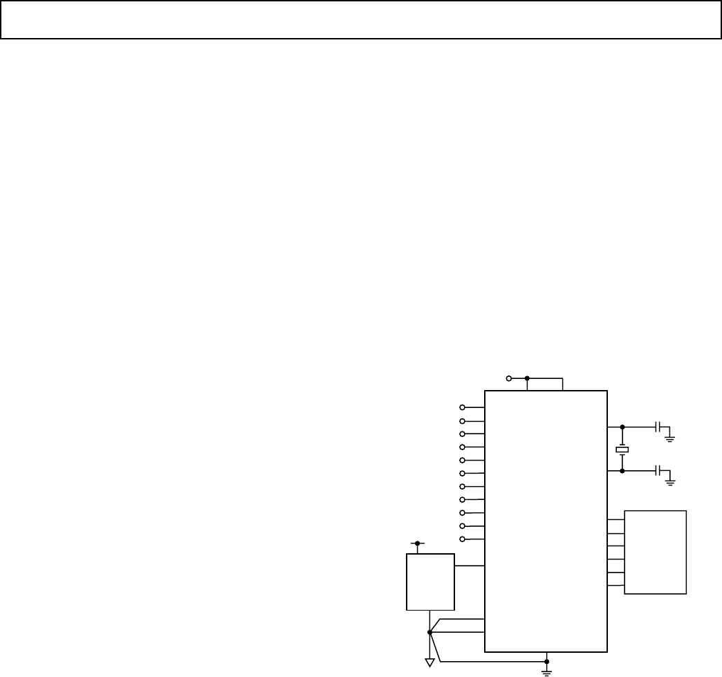
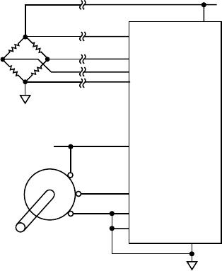
Grounding and Layout
Since the analog inputs and reference inputs are differential,
most of the voltages in the analog modulator are common-mode
voltages. The excellent common-mode rejection of the part will
remove common-mode noise on these inputs. The analog and
digital supplies to the AD7708/AD7718 are independent and
separately pinned out to minimize coupling between the analog
and digital sections of the device. The AD7708/AD7718 can be
operated with 5 V analog and 3 V digital supplies or vice versa.
The digital filter will provide rejection of broadband noise on
the power supplies, except at integer multiples of the modulator
sampling frequency. The digital filter also removes noise from
the analog and reference inputs provided these noise sources do
not saturate the analog modulator. As a result, the AD7708/
AD7718 is more immune to noise interference than a conventional
high-resolution converter. However, because the resolution of the
AD7708/AD7718 is so high and the noise
levels from the
converter so low, care must be taken with regard to grounding
and layout.
The printed circuit board that houses the ADC should be designed
so the analog and digital sections are separated and confined to
certain areas of the board. This facilitates the use of ground planes
that can be easily separated. A minimum etch technique is
generally best for ground planes as it gives the best shielding.
Although the AD7708/AD7718 has separate pins for analog and
digital ground, the AGND and DGND pins are tied together
internally via the substrate. Therefore, the user must not tie
these two pins to separate ground planes unless the ground
planes are connected together near the AD7708/AD7718.
In systems where the AGND and DGND are connected some-
where else in the system, i.e., the systems power supply, they
should not be connected again at the AD7708/AD7718 or a
ground loop will result. In these situations it is recommended that
ground pins of the AD7708/AD7718 be tied to the AGND plane.
In any layout it is implicit that the user keep in mind the flow of
currents in the system, ensuring that the paths for all currents
are as close as possible to the paths the currents took to reach
their destinations. Avoid forcing digital currents to flow through
the AGND.
Avoid running digital lines under the device as these will couple
noise onto the die. The analog ground plane should be allowed
to run under the AD7708/AD7718 to prevent noise coupling.
The power supply lines to the AD7708/AD7718 should use as
wide a trace as possible to provide low impedance paths and
reduce the effects of glitches on the power supply line. Fast
switching signals like clocks should be shielded with digital
ground to avoid radiating noise to other sections of the board
and clock signals should never be run near the analog inputs.
Avoid crossover of digital and analog signals. Traces on opposite
sides of the board should run at right angles to each other. This will
reduce the effects of feedthrough through the board. A microstrip
technique is by far the best, but is not always possible with a
double-sided board. In this technique, the component side of
the board is dedicated to ground planes while signals are placed
on the solder side.
REV. 0
AD7708/AD7718
–41–
Good decoupling is important when using high resolution ADCs.
All analog supplies should be decoupled with 10 µF tantalum in
parallel with 0.1 µF capacitors to AGND. To achieve the best
from these decoupling components, they have to be placed
as close as possible to the device, ideally right up against the
device. All logic chips should be decoupled with 0.1 µF ceramic
capacitors to DGND. In systems where a common supply
voltage is used to drive both the AV
DD
and DV
DD
of the AD7708/
AD7718, it is recommended that the system’s AV
DD
supply is
used. This supply should have the recommended analog supply
decoupling capacitors between the AV
DD
pin of the AD7708/
AD7718 and AGND and the recommended digital supply
decoupling capacitor between the DV
DD
pin of the AD7708/
AD7718 and DGND.
APPLICATIONS
The AD7708/AD7718 provides a low cost, high resolution
analog-to-digital function. The AD7708 offers 16-bit resolution
while the AD7718 offers 24-bit resolution. The AD7708 and
AD7718 are pin and function compatible. The AD7718 allows a
direct upgradable path from a 16-bit to a 24-bit system with
minimal software and no hardware changes. Because the analog-
to-digital function is provided by a sigma-delta architecture, it
makes the part more immune to noisy environments, thus mak-
ing the part ideal for use in sensor measurement and in industrial
and process control applications. There are two modes of operation
associated with the AD7708/AD7718, chop enabled (CHOP = 0)
or chop disabled (CHOP = 1). With chop enabled the signal chain
is chopped and the device is factory-calibrated at final test in
this mode. Field calibration can be avoided due to the extremely
low offset and gain drifts exhibited by the converter in this
mode. While operating in this mode gives optimum performance
in terms of offset error and offset and gain drift performance, it
offers limited throughput when cycling through all channels.
With chopping disabled, the signal chain is not chopped and
therefore the user needs to ensure that the ADC is calibrated on
range changes and if there is a significant temperature change
as the gain and offset drift performance is degraded.
The key advantage in using the AD7708/AD7718 with chopping
disabled is in channel cycling applications where system through-
put is of prime importance. The max conversion rate with chop
disabled is 1.36 kHz compared with 105 Hz with chop enabled.
The AD7708/AD7718 also provides a programmable gain ampli-
fier, a digital filter, and system calibration options. Thus, it
provides far more system level functionality than off-the-shelf
integrating ADCs without the disadvantage of having to sup-
ply a high quality integrating capacitor. In addition, using the
AD7708/AD7718 in a system allows the system designer to
achieve a much higher level of resolution because noise perfor-
mance of the AD7708/AD7718 is significantly better than that
of integrating ADCs.
The on-chip PGA allows the AD7708/AD7718 to handle an
analog input voltage range as low as 10 mV full scale with V
REF
= 1.25 V. The AD7708/AD7718 can be operated in 8-channel
mode with two reference input options or 10-channel mode with
one reference input. Eight-channel mode allows both ratiometric
or absolute measurements to be performed on any channel using
the two reference input options. The differential analog inputs
of the part allow this analog input range to have an absolute
value anywhere between AGND + 100 mV and AV
DD
– 100 mV.
The buffer on the negative analog input can be bypassed allowing
the AD7708/AD7718 be operated as eight or ten single-ended
input channels. The PGA allows the user to connect transducers
directly to the input of the AD7708/AD7718. The program-
mable gain front end on the AD7708/AD7718 allows the part to
handle unipolar analog input ranges from 0 mV to +20 mV to
0 V to +2.5 V and bipolar inputs of ±20 mV to ±2.5 V. Because
the part operates from a single supply these bipolar ranges are
with respect to a biased-up differential input.
Data Acquisition
The AD7708/AD7718, with its different configuration options
(five fully-differential input or 10 pseudo-differential input
channels with one reference input or four fully-differential input
or eight pseudo-differential input channels with two reference
inputs), is suited to low bandwidth, high resolution data acquisi-
tion systems. In addition, the 3-wire digital interface allows this
data acquisition front end to be isolated with just three opto-
isolators. The entire system can be operated from a single 3 V
or 5 V supply, provided that the input signals to the AD7708/
AD7718’s analog inputs are all of positive polarity.
5V
AD780
AIN6
AIN5
AIN4
AIN3
AIN2
AIN1
5V
GND
V
IN
V
OUT
AGND
DGND
AV
DD
DV
DD
REF1IN()
MCLKIN
MCLKOUT
32kHz
AD7708/
AD7718
AIN8
AIN7
AIN9
AINCOM
AIN10
MICRO-
CONTROLLER
SCLK
CS
DIN
DOUT
RDY
RESET
REFIN1(+)
Figure 26. Data Acquisition Using the AD7708/AD7718
Programmable Logic Controllers
The AD7708/AD7718 is also suited to programmable logic
controller applications. In such applications, the ADC is required
to handle signals from a variety of different transducers. The
AD7708/AD7718’s programmable gain front end allows the
part to either handle low level signals directly from a transducer
or full-scale signals that have already been conditioned. The faster
throughput rate and settling time of the part when operated with
chopping disabled makes this the optimum mode of operation in
PLC applications as an important feature in these applications is
loop response time. The configuration of the AD7708/AD7718
in PLC applications is similar to that outlined for a data acquisi-
tion system and is shown in Figure 26. In this application the
AD7708/AD7718 is configured in 10-channel mode, (CHCON
= 1) and can be operated as 10 pseudo-differential inputs with
respect to AINCOM or as five fully-differential input channels.
REV. 0
–42–
AD7708/AD7718
Converting Single-Ended Inputs
The AD7708/AD7718 generally operates in buffered mode. This
places a restriction of AGND + 100 mV to AVDD – 100 mV on
the absolute and common-mode voltages that can be applied to
any input on the AD7708/AD7718.
Some applications may require the measurement of analog
inputs with respect to AGND. To enable the AD7708/AD7718
to be used in these single-ended applications, the buffer on the
AINCOM can be bypassed. The NEGBUF bit in the mode
register controls the operation of the input buffer on the AINCOM
input when a channel is configured for pseudo-differential mode of
operation. If cleared, the analog negative input (AINCOM) is
unbuffered, allowing it to be tied to AGND in single-ended
input configuration. If this bit is set, the analog negative input
(AINCOM) is buffered, placing a restriction on its common-
mode input range. When AINCOM is unbuffered, signals with a
common-mode range from AGND – 30 mV to AVDD + 30 mV
can be accommodated on this input allowing the end user to
connect the AINCOM input to AGND and perform single-
ended measurements with respect to this input. This unbuffered
input path on the AINCOM provides a dynamic load to the
driving source. Therefore, resistor/capacitor combinations on
this input pin can cause dc gain errors, depending on the output
impedance of the source that is driving the AINCOM input. All
analog inputs still operate in buffered mode and their com-
mon-mode and absolute input voltage is restricted to a range
between AGND + 100 mV and AV
DD
– 100 mV.
Combined Ratiometric and Absolute Value Measurement
System
The AD7708/AD7718 when operated with CHCON = 0 can be
configured for operation as four fully-differential analog inputs or
eight pseudo-differential analog inputs with two fully-differential
reference inputs. Having the ability to use either REFIN1 or
REFIN2 with any channel during the conversion process allows
the end user to make both absolute and ratiometric measure-
ments as shown in Figure 27. In this example a fully-differential
analog input (AIN1–AIN2) is being converted from a bridge trans-
ducer in a ratiometric manner using REFIN1 as the reference
input for this channel. AIN3 is configured as a pseudo-differential
input channel using REFIN2 to perform an absolute measurement
on the potentiometer. The REFSEL bit in the mode register is
used to select which reference is used with the active channel
during the conversion process. When the AD7708/AD7718 is
configured with CHCON = 1, only one reference (REFIN1) is
available. The contents of the CHCON bit override the REFSEL
bit. If the ADC is configured in five fully-differential or 10
pseudo-differential input channel mode, the REFSEL bit setting
is irrelevant as only REFIN1 is available.
REFIN1()
AD7718
REFIN2(+)
REFIN1(+)
AINCOM
AIN1
AIN3
AIN2
REFIN2()
GND
EXCITATION VOLTAGE = 4V
WIPER
Figure 27. Absolute and Ratiometric Measurement
System Using AD7718

AD7708BRUZ-REEL

Mfr. #:
Manufacturer:
Analog Devices Inc.
Description:
Analog to Digital Converters - ADC 16-Bit 8/10-Ch Low Vtg Low Pwr
Lifecycle:
New from this manufacturer.
Delivery:
DHL FedEx Ups TNT EMS
Payment:
T/T Paypal Visa MoneyGram Western Union