REV. 0
–34–
AD7708/AD7718
DIGITAL INTERFACE
As previously outlined, the AD7708/AD7718’s programmable
functions are controlled using a set of on-chip registers. Data is
written to these registers via the part’s serial interface and read
access to the on-chip registers is also provided by this interface.
All communications to the part must start with a write operation
to the Communications Register. After power-on or RESET,
the device expects a write to its Communications Register. The
data written to this register determines whether the next operation
to the part is a read or a write operation and also determines to
which register this read or write operation occurs. Therefore,
write access to any of the other registers on the part starts with a
write operation to the Communications Register followed by a
write to the selected register. A read operation from any other
register on the part (including the output data register) starts
with a write operation to the Communications Register followed
by a read operation from the selected register.
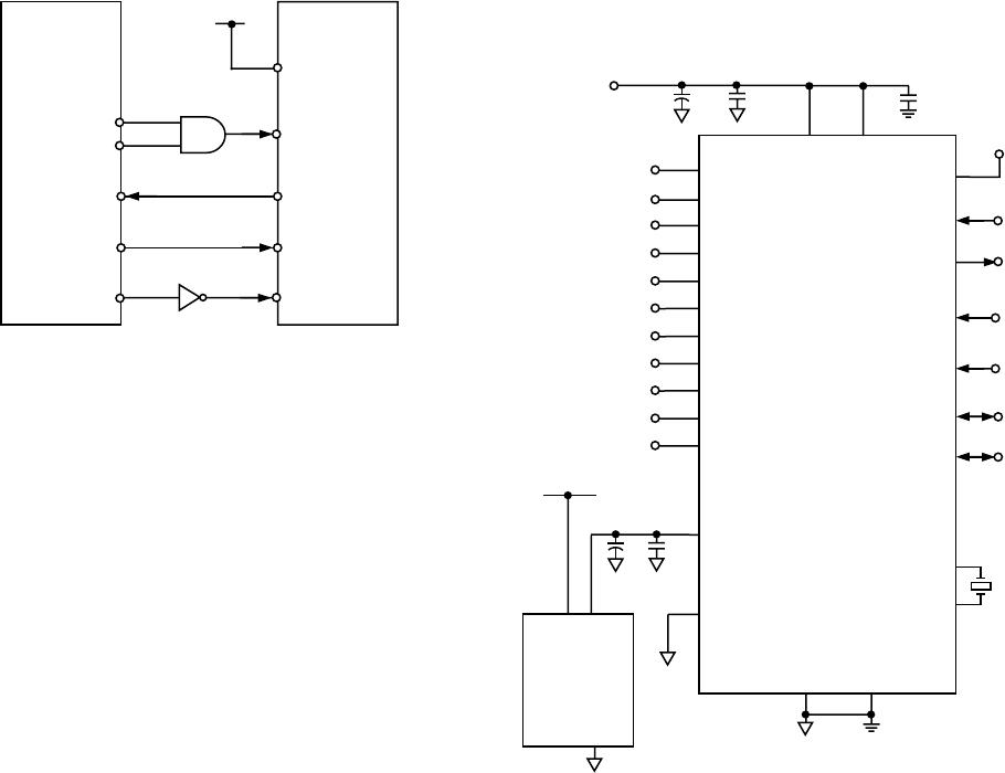
The AD7708/AD7718s serial interface consists of five signals,
CS, SCLK, DIN, DOUT and RDY. The DIN line is used for
transferring data into the on-chip registers while the DOUT line
is used for accessing data from the on-chip registers. SCLK is
the serial clock input for the device and all data transfers (either
on DIN or DOUT) take place with respect to this SCLK signal.
The RDY line is used as a status signal to indicate when data is
ready to be read from the devices’s data register. RDY goes low
when a new data word is available in the output register. It is
reset high when a read operation from the data register is complete.
It also goes high prior to the updating of the output register to
indicate when not to read from the device to ensure that a data
read is not attempted while the register is being updated. CS is
used to select the device. It can be used to decode these devices in
systems where a number of parts are connected to the serial bus.
Figures 2 and 3 show timing diagrams for interfacing to the
AD7708/AD7718 with CS used to decode the part. Figure 3 is
for a read operation from the AD7708/AD7718 output shift
register while Figure 2 shows a write operation to the input shift
register. It is possible to read the same data twice from the out-
put register even though the RDY line returns high after the first
read operation. Care must be taken, however, to ensure that the
read operations have been completed before the next output
update is about to take place.
The serial interface can operate in three-wire mode by tying the
CS input low. In this case, the SCLK, DIN and DOUT lines
are used to communicate with the device and the status of the
RDY bit can be obtained by interrogating the STATUS Regis-
ter. This scheme is suitable for interfacing to microcontrollers. If
CS is required as a decoding signal, it can be generated from a
port bit. For microcontroller interfaces, it is recommended that
the SCLK idles high between data transfers.
The AD7708/AD7718 can also be operated with CS used as a
frame synchronization signal. This scheme is suitable for DSP
interfaces. In this case, the first bit (MSB) is effectively clocked
out by CS since CS would normally occur after the falling edge
of SCLK in DSPs. The SCLK can continue to run between
data transfers provided the timing numbers are obeyed.
The serial interface can be reset by exercising the RESET input
on the part. It can also be reset by writing a series of 1s on the
DIN input. If a Logic 1 is written to the AD7708/AD7718 DIN
line for at least 32 serial clock cycles, the serial interface is reset.
This ensures that in three-wire systems, if the interface is lost
either via a software error or by some glitch in the system, it can
be reset back to a known state. This state returns the interface
to where the ADC is expecting a write operation to its Commu-
nications Register. This operation resets the contents of all
registers to their power-on-reset values.
Some microprocessor or microcontroller serial interfaces have a
single serial data line. In this case, it is possible to connect the
ADC’s DOUT and DIN lines together and connect them to the
single data line of the processor. A 10 kΩ pull-up resistor should
be used on this single data line. In this case, if the interface is
lost, because the read and write operations share the same line,
the procedure to reset it back to a known state is somewhat
different than previously described. It requires a read operation
of 24 serial clocks followed by a write operation where a Logic
1 is written for at least 32 serial clock cycles to ensure that the
serial interface is back into a known state.
MICROCOMPUTER/MICROPROCESSOR INTERFACING
The flexible serial interface allows for easy interface to most
microcomputers and microprocessors. The flowcharts of Figures
16, 17, and 18 outline the sequence that should be followed
when interfacing a microcontroller or microprocessor to the
AD7708/AD7718. Figures 19, 20, and 21 show some typical
interface circuits.
The serial interface on the AD7708/AD7718 is capable of oper-
ating from just three wires and is compatible with SPI interface
protocols. The three-wire operation makes the part ideal for
isolated systems where minimizing the number of interface lines
minimizes the number of opto-isolators required in the system.
The serial clock input is a Schmitt-triggered input to accommo-
date slow edges from optocouplers. The rise and fall times of
other digital inputs to the AD7708/AD7718 should be no slower
than 1 µs.
Most of the registers on the AD7708/AD7718 are 8-bit regis-
ters, which facilitates easy interfacing to the 8-bit serial ports of
microcontrollers. The Data Register on the AD7718 is 24 bits
wide, the ADC data register on the AD7708 is 16 bits wide, and
the offset and gain registers are 16-bit registers on the AD7708
and 24-bit registers on the AD7718; however, data transfers to
these registers can consist of multiple 8-bit transfers to the serial
port of the microcontroller. DSP processors and microproces-
sors generally transfer 16 bits of data in a serial data operation.
Some of these processors, such as the ADSP-2105, have the
facility to program the amount of cycles in a serial transfer. This
allows the user to tailor the number of bits in any transfer to
match the register length of the required register in the AD7708/
AD7718.
Even though some of the registers on the AD7708/AD7718 are
only eight bits in length, communicating with two of these
registers in successive write operations can be handled as a
single 16-bit data transfer if required. For example, if the Filter
Register is to be updated, the processor must first write to the
Communications Register (saying that the next operation is a
write to the Filter Register) and then write eight bits to the Filter
Register. If required, this can all be done in a single 16-bit
transfer because once the eight serial clocks of the write opera-
tion to the Communications Register have been completed,
the part immediately sets itself up for a write operation to the
Filter Register.