REV. 0
–28–
AD7708/AD7718
Operating Characteristics when Addressing the Mode and Control Registers
1. Any change to the MD bits will immediately reset the ADCs. A write to the MD2–MD0 bits with no change is also treated as a reset.
2. Once the MODE has been written with a calibration mode, the RDY bit (STATUS) is immediately reset and the calibration
commences. On completion the appropriate calibration registers are written, the bit in STATUS register is updated and the
MD2–MD0 bits are reset to 001 to indicate the ADC is back in idle mode.
3. Calibrations are performed with the maximum allowable SF value with chop enabled. SF register is reset to user configuration
after calibration with chop enabled. Calibrations are performed with the selected value of SF when chop is disabled.
ADC Control Register (ADCCON): (A3, A2, A1, A0 = 0, 0, 1, 0; Power-On-Reset = 07 Hex)
The ADC Control Register is an 8-bit register from which data can be read or to which data can be written. This register is used to
configure the ADC for range, channel selection, and unipolar or bipolar coding. Table XVI outlines the bit designations for the ADC
control register ADCCON7 through ADCCON0 indicate the bit location, ADCCON denoting the bits are in the ADC Control
Register. ADCCON7 denotes the first bit of the data stream. The number in brackets indicates the power-on/reset default status of
that bit.
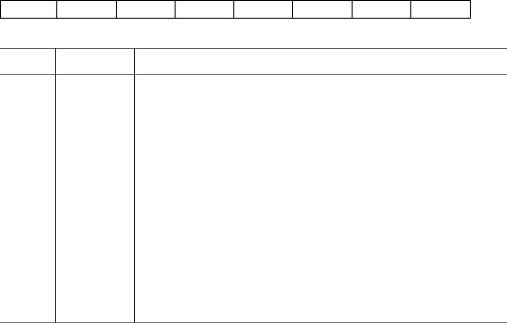
Table XVI. ADC Control Register (ADCCON) Bit Designations
Bit Bit
Location Mnemonic Description
ADCCON7 CH3 ADC Channel Selection Bits. Written by the user to select either pseudo-differential or fully-
ADCCON6 CH2 differential input pairs used by the ADC as follows:
ADCCON5 CH1
ADCCON4 CH0
8-Channel Configuration 10-Channel Configuration
(CHCON = 0) (CHCON = 1)
Positive Negative Cal Register Positive Negative Cal Register
CH3 CH2 CH1 CH0 Input Input Pair Input Input Pair
0 0 0 0 AIN1 AINCOM 1 AIN1 AINCOM 1
0 0 0 1 AIN2 AINCOM 2 AIN2 AINCOM 2
0 0 1 0 AIN3 AINCOM 3 AIN3 AINCOM 3
0 0 1 1 AIN4 AINCOM 4 AIN4 AINCOM 4
0 1 0 0 AIN5 AINCOM 1 AIN5 AINCOM 5
0 1 0 1 AIN6 AINCOM 2 AIN6 AINCOM 1
0 1 1 0 AIN7 AINCOM 3 AIN7 AINCOM 2
0 1 1 1 AIN8 AINCOM 4 AIN8 AINCOM 3
1 0 0 0 AIN1 AIN2 1 AIN1 AIN2 1
1 0 0 1 AIN3 AIN4 2 AIN3 AIN4 2
1 0 1 0 AIN5 AIN6 3 AIN5 AIN6 3
1 0 1 1 AIN7 AIN8 4 AIN7 AIN8 4
1 1 0 0 AIN2 AIN2 1 AIN9 AIN10 5
1 1 0 1 AINCOM AINCOM 1 AINCOM AINCOM 1
1 1 1 0 REFIN(+) REFIN(–) 1 AIN9 AINCOM 4
1 1 1 1 OPEN OPEN 1 AIN10 AINCOM 5
ADCCON3 U/B Unipolar/Bipolar Bit.
Set by user to enable unipolar coding i.e., zero differential input will result in 000000hex
output and a full-scale differential input will result in FFFFFF Hex output when operated in
24-bit mode.
Cleared by user to enable bipolar coding, Negative full-scale differential input will result in an
output code of 000000 Hex, zero differential input will result in an output code of 800000 Hex
and a positive full-scale differential input will result in an output code of FFFFFF Hex.
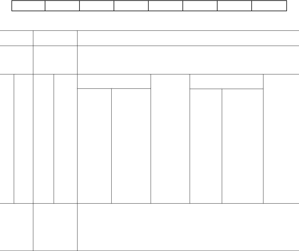
ADCCON7 ADCCON6 ADCCON5 ADCCON4 ADCCON3 ADCCON2 ADCCON1 ADCCON0
CH3 (0) CH2 (0) CH1 (0) CH0 (0) U/B (0) RN2 (1) RN1 (1) RN0 (1)