REV. 0
AD7708/AD7718
–19–
SIGNAL CHAIN OVERVIEW CHOP DISABLED
(CHOP = 1)
With CHOP =1 chopping is disabled. With chopping disabled
the available output rates vary from 16.06 Hz (62.26 ms) to
1365.33 Hz (0.73 ms). The range of applicable SF words is from
3 to 255. When switching between channels with chop disabled,
the channel throughput is increased by a factor of two over the
case where chop is enabled. When used in multiplexed applica-
tions operation with chop disabled will offer the best throughput
time when cycling through all channels. The drawback with
chop disabled is that the drift performance is degraded and
calibration is required following a gain change or significant
temperature change. A block diagram of the ADC input
channel with chop disabled is shown in Figure 10. The
signal chain includes a mux, buffer, PGA, sigma-delta modu-
lator, and digital filter. The modulator bit stream is applied to
a Sinc
3
filter. The programming of the Sinc
3
decimation
factor is restricted to an 8-bit register SF, the actual decima-
tion factor is the register value times 8. The decimated output
rate from the Sinc
3
filter (and the ADC conversion rate) will there-
fore be:
f
f
SF
ADC
MOD
=
×8
where
f
ADC
is the ADC conversion rate,
SF is the decimal equivalent of the word loaded to the filter
register, valid range is from 3 to 255,
f
MOD
is the modulator sampling rate of 32.768 kHz.
The settling time to a step input is governed by the digital filter.
A synchronized step change will require a settling time of three
times the programmed update rate, a channel change can be
treated as a synchronized step change. An unsynchronized step
change will require four outputs to reflect the new analog input
at its output.
t
f
t
SETTLE
ADC
ADC
==×
3
3
The allowable range for SF is 3 to 255 with a default of 69
(45H). The corresponding conversion rates, conversion times,
and settling times are shown in Table VI. Note that the conver-
sion time increases by 0.245 ms for each increment in SF.
Table VI. ADC Conversion and Settling Times for Various
SF Words with CHOP = 1
SF Data Update Rate Settling Time
Word f
ADC
(Hz) t
SETTLE
(ms)
03 1365.33 2.20
68 60.2 49.8
69 (Default) 59.36 50.54
75 54.6 54.93
82 49.95 60
151 27.13 110.6
255 16.06 186.76
The frequency response of the digital filter H (f) is as follows:
1
8
8
3
SF
SF f f
ff
MOD
MOD
×
×
×× ×
×
sin( / )
sin( / )
π
π
where
f
MOD
= 32,768 Hz,
SF = value programmed into SF SFR.
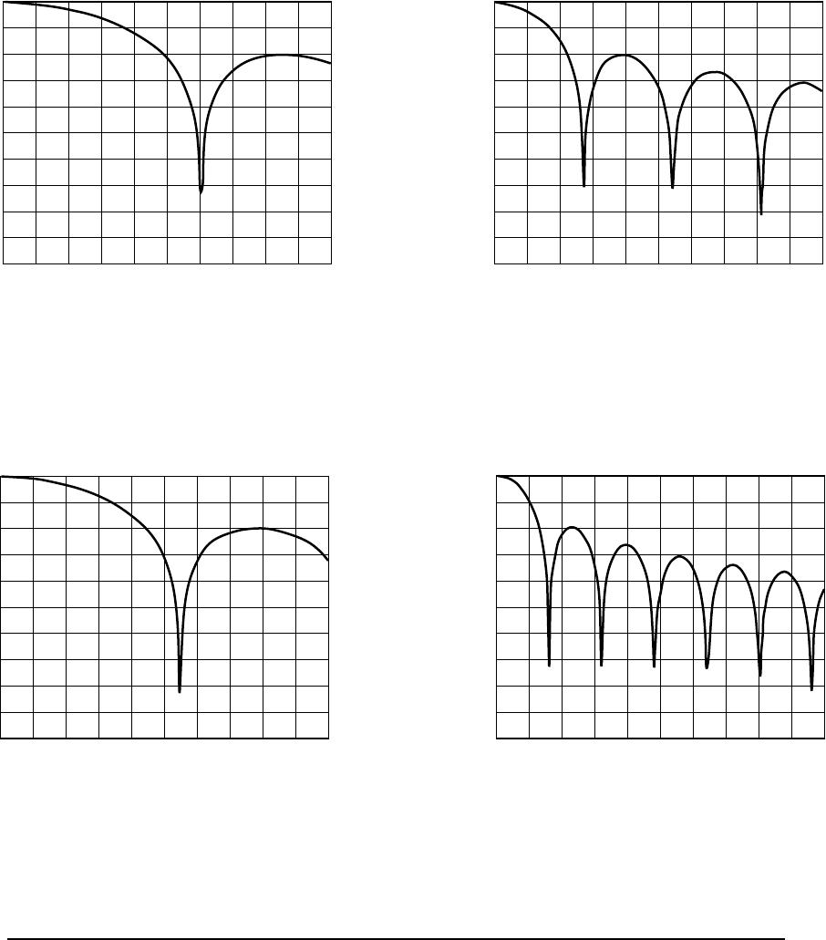
The following shows plots of the filter frequency response using
different SF words for output data rates
of 16 Hz to 1.36 kHz.
There are sinc
3
notches at integer multiples of the update rate.
The 3 dB frequency for all values of SF obeys the following
equation:
f (3 dB) = 0.262 × f
ADC
The following plots show frequency response of the AD7708/
AD7718 digital filter for various filter words. The AD7708/
AD7718 are targeted at multiplexed applications. One of the
key requirements in these applications is to optimize the SF
word to obtain the maximum filter rejection at 50 Hz and 60 Hz
while minimizing the channel throughput rate. Figure 12 shows
the AD7708/AD7718 optimized throughput while maximizing
50 Hz and 60 Hz rejection. This is achieved with an SF word of
75. In Figure 13, by using a higher SF word of 151, 50 Hz and
60 Hz rejection can be maximized at 60 dB with a channel
throughput rate of 110 ms. An SF word of 255 gives maximum
rejection at both 50 Hz and 60 Hz but the channel throughput
rate is restricted to 186 ms as shown in Figure 14.
SINC
3
FILTER
MUX
BUF
PGA
-
MOD0
ANALOG
INPUT
DIGITAL
OUTPUT
f
IN
f
MOD
f
ADC
Figure 10. ADC Channel Block Diagram with CHOP Disabled
REV. 0
–20–
AD7708/AD7718
FREQUENCY Hz
0
80
160
0 10010
ATTENUATION dB
20 30 40 50 60 70 80 90
20
40
120
140
60
100
SF = 68
OUTPUT DATA RATE = 60.2Hz
SETTLING TIME = 49.8ms
INPUT BANDWIDTH = 15.5Hz
50Hz REJECTION = 43dB, 50Hz1Hz REJECTION = 40dB
60Hz REJECTION = 147dB, 60Hz1Hz REJECTION = 101dB
200
180
Figure 11. Frequency Response Operating with the
SF Word of 68
FREQUENCY Hz
0
80
160
0 10010
ATTENUATION dB
20 30 40 50 60 70 80 90
20
40
120
140
60
100
SF = 75
OUTPUT DATA RATE = 54.6Hz
SETTLING TIME = 55ms
INPUT BANDWIDTH = 14.3Hz
50Hz REJECTION = 62.5dB, 50Hz1Hz REJECTION = 57dB
60Hz REJECTION = 63dB, 60Hz1Hz REJECTION = 60dB
200
180
Figure 12. Optimizing Filter Response for Throughput
while Maximizing the Simultaneous 50 Hz and 60 Hz
Rejection
FREQUENCY Hz
0
80
160
0 10010
ATTENUATION dB
20 30 40 50 60 70 80 90
20
40
120
140
60
100
SF = 151
OUTPUT DATA RATE = 27.12Hz
SETTLING TIME = 110ms
INPUT BANDWIDTH = 27.12Hz
50Hz REJECTION = 65.4dB, 50Hz1Hz REJECTION = 60dB
60Hz REJECTION = 63dB, 60Hz1Hz REJECTION = 60dB
200
180
Figure 13. Optimizing Filter Response for Maximum
Simultaneous 50 Hz and 60 Hz Rejection
FREQUENCY Hz
0
80
160
0 10010
ATTENUATION dB
20 30 40 50 60 70 80 90
20
40
120
140
60
100
SF = 255
OUTPUT DATA RATE = 16.06Hz
SETTLING TIME = 186ms
INPUT BANDWIDTH = 4.21Hz
50Hz REJECTION = 87dB, 50Hz1Hz REJECTION = 77dB
60Hz REJECTION = 72dB, 60Hz1Hz REJECTION = 68dB
200
180
Figure 14. Frequency with Maximum SF Word = 255
ADC NOISE PERFORMANCE CHOP DISABLED
(CHOP = 1)
Tables VII to X show the output rms noise and output peak-to-
peak resolution in bits (rounded to the nearest 0.5 LSB) for
some typical output update rates. The numbers are typical and
generated at a differential input voltage of 0 V. The output update
rate is selected via the SF7–SF0 bits in the Filter Register. It is
important to note that the peak-to-peak resolution figures represent
the resolution for which there will be no code flicker within a
six-sigma limit. The output noise comes from two sources. The
first is the electrical noise in the semiconductor devices (device
noise) used in the implementation of the modulator. Secondly,
when the analog input is converted into the digital domain,
quantization noise is added. The device noise is at a low level
and is independent of frequency. The quantization noise starts
at an even lower level but rises rapidly with increasing frequency
to become the dominant noise source. The numbers in the
tables are given for the bipolar input ranges. For the unipolar
ranges the rms noise numbers will be the same as the bipolar
range, but the peak-to-peak resolution is now based on half the
signal range which effectively means losing 1 bit of resolution.
REV. 0
AD7708/AD7718
–21–
Table VII. Typical Output RMS Noise vs. Input Range and Update Rate for AD7718 with Chop Disabled (CHOP = 1);
Output RMS Noise in V
SF Data Update
Input Range
Word Rate (Hz) 20 mV 40 mV 80 mV 160 mV 320 mV 640 mV 1.28 V 2.56 V
03 1365.33 30.31 29.02 58.33 112.7 282.44 361.72 616.89 1660
13 315.08 2.47 2.49 2.37 3.87 7.18 12.61 16.65 32.45
66 62.06 0.743 0.852 0.9183 0.8788 0.8795 1.29 1.99 3.59
69 59.38 0.961 0.971 0.949 0.922 0.923 1.32 2.03 3.73
81 50.57 0.894 0.872 0.872 0.806 0.793 1.34 2.18 2.96
255 16.06 0.475 0.468 0.434 0.485 0.458 0.688 1.18 1.78
Table VIII. Peak-to-Peak Resolution vs. Input Range and Update Rate for AD7718 with Chop Disabled (CHOP = 1);
Peak-to-Peak Resolution in Bits
SF Data Update
Input Range
Word Rate (Hz) 20 mV 40 mV 80 mV 160 mV 320 mV 640 mV 1.28 V 2.56 V
03 1365.33 8999 9 9 9 9
13 315.08 11 12 14 14 14 14 15 15
66 62.06 13 14 15 16 17 17 18 18
69 59.36 13 14 15 16 17 17 18 18
81 50.57 13 14 15 16 17 17 18 18
255 16.06 14 15 16 17 18 18 19 19
Table IX. Typical Output RMS Noise vs. Input Range and Update Rate for AD7708 with Chop Disabled (CHOP = 1);
Output RMS Noise in V
SF Data Update
Input Range
Word Rate (Hz) 20 mV 40 mV 80 mV 160 mV 320 mV 640 mV 1.28 V 2.56 V
03 1365.33 30.31 29.02 58.33 112.7 282.44 361.72 616.89 1660
13 315.08 2.47 2.49 2.37 3.87 7.18 12.61 16.65 32.45
66 62.06 0.743 0.852 0.9183 0.8788 0.8795 1.29 1.99 3.59
69 59.38 0.961 0.971 0.949 0.922 0.923 1.32 2.03 3.73
81 50.57 0.894 0.872 0.872 0.806 0.793 1.34 2.18 2.96
255 16.06 0.475 0.468 0.434 0.485 0.458 0.688 1.18 1.78
Table X. Peak-to-Peak Resolution vs. Input Range and Update Rate for AD7708 with Chop Disabled (CHOP = 1);
Peak-to-Peak Resolution in Bits
SF Data Update
Input Range
Word Rate (Hz) 20 mV 40 mV 80 mV 160 mV 320 mV 640 mV 1.28 V 2.56 V
03 1365.33 8999 9 9 9 9
13 315.08 11 12 14 14 14 14 15 15
66 62.06 13 14 15 16 16 16 16 16
69 59.36 13 14 15 16 16 16 16 16
81 50.57 13 14 15 16 16 16 16 16
255 16.06 14 15 16 16 16 16 16 16

AD7708BRUZ-REEL

Mfr. #:
Manufacturer:
Analog Devices Inc.
Description:
Analog to Digital Converters - ADC 16-Bit 8/10-Ch Low Vtg Low Pwr
Lifecycle:
New from this manufacturer.
Delivery:
DHL FedEx Ups TNT EMS
Payment:
T/T Paypal Visa MoneyGram Western Union