REV. 0
AD7708/AD7718
–17–
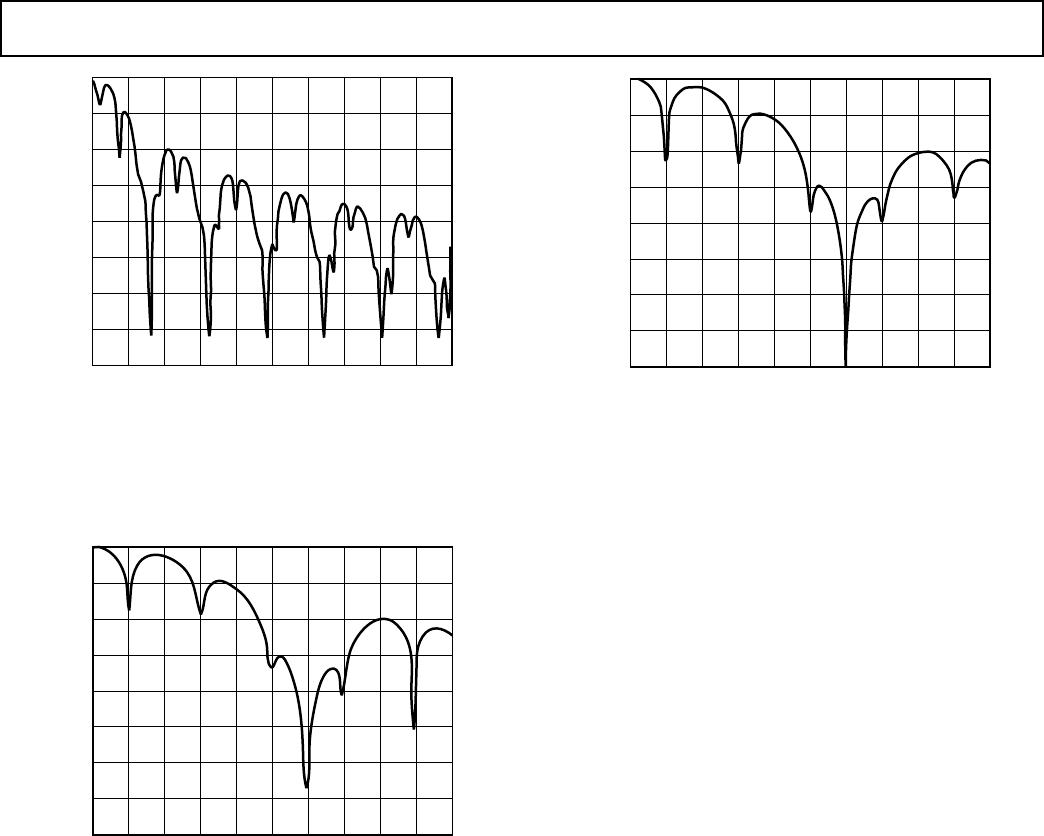
FREQUENCY – Hz
0
–80
–160
0 10010
ATTENUATION – dB
20 30 40 50 60 70 80 90
–20
–40
–120
–140
–60
–100
SF = 255
OUTPUT DATA RATE = 5.35Hz
INPUT BANDWIDTH = 1.28Hz
50Hz REJECTION = –93dB, 50Hzⴞ1Hz REJECTION = –93dB
60Hz REJECTION = –74dB, 60Hzⴞ1Hz REJECTION = –68dB
Figure 7. Filter Profile with SF = 255
FREQUENCY – Hz
0
–80
–160
0 100
10
ATTENUATION – dB
20 30 40 50 60 70 80 90
–20
–40
–120
–140
–60
–100
SF = 69
OUTPUT DATA RATE = 19.8Hz
INPUT BANDWIDTH = 4.74Hz
FIRST NOTCH = 9.9Hz
50Hz REJECTION = –66dB, 50Hzⴞ1Hz REJECTION = –60dB
60Hz REJECTION = –117dB, 60Hzⴞ1Hz REJECTION = –94dB
Figure 8. Filter Profile with Default SF = 69 Giving Filter
Notches at Both 50 Hz and 60 Hz
FREQUENCY – Hz
0
–80
–160
0 10010
ATTENUATION – dB
20 30 40 50 60 70 80 90
–20
–40
–120
–140
–60
–100
SF = 68
OUTPUT DATA RATE = 20.07Hz
INPUT BANDWIDTH = 4.82Hz
50Hz REJECTION = –74dB, 50Hzⴞ1Hz REJECTION = –54.6dB
60Hz REJECTION = –147dB, 60Hzⴞ1Hz REJECTION = –101dB
Figure 9. Filter Profile with SF = 68
ADC NOISE PERFORMANCE CHOP ENABLED
(CHOP = 0)
Tables II to V show the output rms noise and output peak-to-
peak resolution in bits (rounded to the nearest 0.5 LSB) for a
selection of output update rates. The numbers are typical and
generated at a differential input voltage of 0 V with AV
DD
=
DV
DD
= 5 V and using a 2.5 V reference. The output update
rate is selected via the SF7–SF0 bits in the Filter Register. It is
important to note that the peak-to-peak resolution figures repre-
sent the resolution for which there will be no code flicker within
a six-sigma limit. The output noise comes from two sources. The
first is the electrical noise in the semiconductor devices (device
noise) used in the implementation of the modulator. Secondly,
when the analog input is converted into the digital domain,
quantization noise is added. The device noise is at a low level
and is independent of frequency. The quantization noise starts at
an even lower level but rises rapidly with increasing frequency to
become the dominant noise source. The numbers in the tables
are given for the bipolar input ranges. For the unipolar ranges
the rms noise numbers will be the same as the bipolar range, but
the peak-to-peak resolution is now based on half the signal range
which effectively means losing one bit of resolution.

