AD7705/AD7706
Rev. C | Page 10 of 44
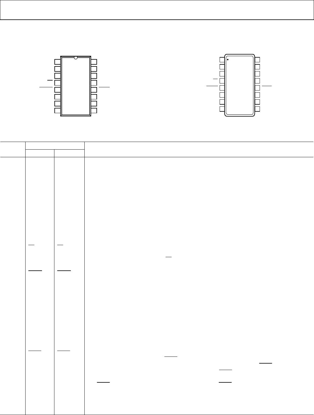
PIN CONFIGURATIONS AND FUNCTION DESCRIPTIONS
SCLK
1
MCLK IN
2
MCLK OUT
3
CS
4
GND
16
V
DD
15
DIN
14
DOUT
13
RESET
5
DRDY
12
AIN2(+)
6
AIN2(–)
11
AIN1(+)
7
REF IN(–)
10
AIN1(–)
8
REF IN(+)
9
AD7705
TOP VIEW
(Not to Scale)
01166-003
Figure 3. AD7705 Pin Configuration
1
2
3
4
5
6
7
8
16
15
14
13
12
11
10
9
MCLK IN
MCLK OUT
CS
AIN2
AIN1
RESET
SCLK
V
DD
DIN
DOUT
REF IN(–)
COMMON REF IN(+)
AIN3
DRDY
GND
AD7706
TOP VIEW
(Not to Scale)
01166-004
Figure 4. AD7706 Pin Configuration
Table 4. Pin Function Descriptions
Mnemonic
Pin No. AD7705 AD7706 Description
1 SCLK SCLK
Serial Clock. An external serial clock is applied to the Schmitt-triggered logic input to access serial
data from the AD7705/AD7706. This serial clock can be a continuous clock with all data transmitted in
a continuous train of pulses. Alternatively, it can be a noncontinuous clock with the information
transmitted to the AD7705/AD7706 in smaller batches of data.
2 MCLK IN MCLK IN
Master Clock Signal. This can be provided in the form of a crystal/resonator or external clock. A
crystal/resonator can be tied across the Pin MCLK IN and Pin MCLK OUT. Alternatively, the MCLK IN
pin can be driven with a CMOS-compatible clock with the MCLK OUT pin left unconnected. The parts
can be operated with clock frequencies in the range of 500 kHz to 5 MHz.
3 MCLK OUT MCLK OUT
When the master clock for these devices is a crystal/resonator, the crystal/resonator is connected
between Pin MCLK IN and Pin MCLK OUT. If an external clock is applied to Pin MCLK IN, Pin MCLK OUT
provides an inverted clock signal. This clock can be used to provide a clock source for external
circuitry and is capable of driving 1 CMOS load. If the user does not require this clock externally, Pin
MCLK OUT can be turned off via the CLKDIS bit of the clock register. This ensures that the part does
not unnecessarily burn power driving capacitive loads on Pin MCLK OUT.
4
CS
CS Chip Select. Active low logic input used to select the AD7705/AD7706. With this input hardwired low,
the AD7705/AD7706 can operate in its 3-wire interface mode with Pin SCLK, Pin DIN, and Pin DOUT
used to interface to the device. The CS
pin can be used to select the device communicating with the
AD7705/AD7706.
5
RESET
RESET Logic Input. Active low input that resets the control logic, interface logic, calibration coefficients,
digital filter, and analog modulator of the parts to power-on status.
6 AIN2(+) AIN1 Positive Input of the Differential Analog Input Pair AIN2(+)/AIN2(−) for AD7705. Channel 1 for AD7706.
7 AIN1(+) AIN2 Positive Input of the Differential Analog Input Pair AIN1(+)/AIN1(−) for AD7705. Channel 2 for AD7706.
8 AIN1(−) COMMON
Negative Input of the Differential Analog Input Pair AIN1(+)/AIN1(−) for AD7705. COMMON input for
AD7706 with Channel 1, Channel 2, and Channel 3 referenced to this input.
9 REF IN(+) REF IN(+)
Reference Input. Positive input of the differential reference input to the AD7705/AD7706. The reference
input is differential with the provision that REF IN(+) must be greater than REF IN(−).
REF IN(+) can lie anywhere between V
DD
and GND.
10 REF IN(−) REF IN(−)
Reference Input. Negative input of the differential reference input to the AD7705/AD7706. The
REF IN(−) can lie anywhere between V
DD
and GND, provided that REF IN(+) is greater than REF IN(−).
11 AIN2(−) AIN3 Negative Input of the Differential Analog Input Pair AIN2(+)/AIN2(−) for AD7705. Channel 3 for AD7706.
12
DRDY
DRDY Logic Output. A logic low on this output indicates that a new output word is available from the
AD7705/AD7706 data register. The DRDY
pin returns high upon completion of a read operation of a
full output word. If no data read has taken place between output updates, the DRDY
line returns high
for 500 × t
CLK IN
cycles prior to the next output update. While DRDY is high, a read operation should
neither be attempted nor in progress to avoid reading from the data register as it is being updated.
The DRDY
line returns low after the update has taken place. DRDY is also used to indicate when the
AD7705/AD7706 has completed its on-chip calibration sequence.
13 DOUT DOUT
Serial Data Output. Serial data is read from the output shift register on the part. The output shift
register can contain information from the setup register, communication register, clock register, or
data register, depending on the register selection bits of the communication register.

