AD7705/AD7706
Rev. C | Page 28 of 44
THEORY OF OPERATION
CLOCKING AND OSCILLATOR CIRCUIT
The AD7705/AD7706 each require a master clock input, which
can be an external CMOS-compatible clock signal applied to
the MCLK IN pin with the MCLK OUT pin left unconnected.
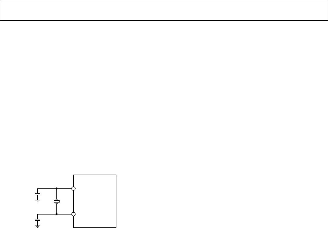
Alternatively, a crystal or ceramic resonator of the correct
frequency can be connected between MCLK IN and
MCLK OUT, as shown in
Figure 17. In this case, the clock
circuit functions as an oscillator, providing the clock source for
the part. The input sampling frequency, modulator sampling
frequency, –3 dB frequency, output update rate, and calibration
time are directly related to the master clock frequency, f
CLKIN
.
Reducing the master clock frequency by a factor of two halves
the above frequencies and update rate and doubles the
calibration time. The current drawn from the V
DD
power supply
is also related to f
CLKIN
. Reducing f
CLKIN
by a factor of two halves
the digital part of the total V
DD
current, but does not affect the
current drawn by the analog circuitry.
MCLK IN
MCLK OUT
CRYSTAL OR
CERAMIC
RESONATOR
C1
C2
AD7705/AD7706
01166-017
Figure 17. Crystal/Resonator Connection for the AD7705/AD7706
Using the part with a crystal or ceramic resonator between the
MCLK IN pin and MCLK OUT pin generally causes more
current to be drawn from V
DD
than does clocking the part from
a driven clock signal at the MCLK IN pin. This is because the
on-chip oscillator circuit is active in the case of the crystal or
ceramic resonator. Therefore, the lowest possible current on the
AD7705/AD7706 is achieved with an externally applied clock at
the MCLK IN pin with MCLK OUT unconnected, unloaded, and
disabled.
The amount of additional current taken by the oscillator
depends on a number of factors. For example, the larger the
value of the capacitor (C1 and C2) placed on the MCLK IN and
MCLK OUT pins, the larger the current consumption on the
AD7705/AD7706. To avoid unnecessarily consuming current,
care should be taken not to exceed the capacitor values
recommended by the crystal and ceramic resonator manufac-
turers. Typical values for C1 and C2 are recommended by
crystal or ceramic resonator manufacturers, usually in the range
of 30 pF to 50 pF. If the capacitor values on MCLK IN and
MCLK OUT are kept in this range, they do not result in any
excessive current. Another factor that influences the current is
the effective series resistance (ESR) of the crystal that appears
between the MCLK IN and MCLK OUT pins of the AD7705/
AD7706. As a general rule, the lower the ESR value, the lower
the current taken by the oscillator circuit.
When operating with a clock frequency of 2.4576 MHz, there is
a 50 μA difference in the current between an externally applied
clock and a crystal resonator operated with a V
DD
of 3 V. With
V
DD
= 5 V and f
CLKIN
= 2.4576 MHz, the typical current increases
by 250 μA for a crystal- or resonator-supplied clock vs. an
externally applied clock. The ESR values for crystals and
resonators at this frequency tend to be low, and, as a result,
there tends to be little difference between different crystal and
resonator types.
When operating with a clock frequency of 1 MHz, the ESR
value for different crystal types varies significantly. As a result,
the current drain varies across crystal types. When using a crystal
with an ESR of 700 Ω, or when using a ceramic resonator, the
increase in the typical current over an externally applied clock is
20 μA with V
DD
= 3 V, and 200 μA with V
DD
= 5 V. When using
a crystal with an ESR of 3 kΩ, the increase in the typical current
over an externally applied clock is 100 μA with V
DD
= 3 V, but
400 μA with V
DD
= 5 V.
There is a start-up time before the on-chip oscillator circuit
oscillates at its correct frequency and voltage levels. Typical start-
up times with V
DD
= 5 V are 6 ms using a 4.9512 MHz crystal,
16 ms with a 2.4576 MHz crystal, and 20 ms with a 1 MHz crystal
oscillator. Start-up times are typically 20% slower when a 3 V
power supply is used. With 3 V supplies, depending on the loading
capacitances on the MCLK pins, a 1 MΩ feedback resistor might
be required across the crystal or resonator to keep the start-up
times around 20 ms.
The AD7705/AD7706 master clock appears on the MCLK OUT
pin of the device. The maximum recommended load on this pin
is 1 CMOS load. When using a crystal or ceramic resonator to
generate the AD7705/AD7706 clock, it might be desirable to
use this clock as the clock source for the system. In this case, it
is recommended that the MCLK OUT signal be buffered with a
CMOS buffer before being applied to the rest of the circuit.
SYSTEM SYNCHRONIZATION
The FSYNC bit of the setup register allows the user to reset the
modulator and digital filter without affecting the setup conditions
on the part. This allows the user to start gathering samples of the
analog input at a known point in time, that is, when the FSYNC
changes from 1 to 0.
With a 1 in the FSYNC bit of the setup register, the digital filter
and analog modulator are held in a known reset state, and the
part does not process input samples. When a 0 is written to the
FSYNC bit, the modulator and filter are taken out of this reset
state, and the part resumes gathering samples on the next
master clock edge.
AD7705/AD7706
Rev. C | Page 29 of 44
The FSYNC input can also be used as a software start convert
command, allowing the AD7705/AD7706 to be operated in a
conventional converter fashion. In this mode, writing to the
FSYNC bit starts conversion, and the falling edge of
DRDY
indicates when conversion is complete. The disadvantage of this
scheme is that the settling time of the filter must be taken into
account for every data register update; therefore, the rate at which
the data register is updated is three times slower in this mode.
Because the FSYNC bit resets the digital filter, the full settling
time of 3 × 1/output rate must elapse before a new word is
loaded to the output register. If the
DRDY
signal is low when
FSYNC goes to 0, the
DRDY
signal is not reset to high by the
FSYNC command, because the AD7705/AD7706 recognize that
there is a word in the data register that has not been read. The
DRDY
line stays low until an update of the data register takes
place, at which time it goes high for 500 × t
CLKIN
before returning
low again. A read from the data register resets the
DRDY
signal
high, and it does not return low until the settling time of the
filter has elapsed and there is a valid new word in the data register.
If the
DRDY
line is high when the FSYNC command is issued,
the
DRDY
line does not return low until the settling time of the
filter has elapsed.
RESET INPUT
The
RESET
input on the AD7705/AD7706 resets the logic, digital
filter, analog modulator, and on-chip registers to their default states.
DRDY
is driven high, and the AD7705/AD7706 ignore all
communication to their registers while the
RESET
input is low.
When the
RESET
input returns high, the AD7705/AD7706 start
to process data, and
DRDY
returns low in 3 × 1/output rate,
indicating a valid new word in the data register. However, the
AD7705/AD7706 operate with their default setup conditions
after a reset, and it is generally necessary to set up all registers
and perform a calibration after a
RESET
command.
The AD7705/AD7706 on-chip oscillator circuit continues to
function even when the
RESET
input is low, and the master
clock signal continues to be available on the MCLK OUT pin.
Therefore, in applications where the system clock is provided by
the AD7705/AD7706 clock, the AD7705/AD7706 produce an
uninterrupted master clock during a
RESET
command.
STANDBY MODE
The STBY bit in the communication register of the AD7705/
AD7706 allows the user to place the part in a power-down
mode when it is not required to provide conversion results. The
AD7705/AD7706 retain the contents of their on-chip registers,
including the data register, while in standby mode. When released
from standby mode, the parts start to process data, and a new
word is available in the data register in 3 × 1/output rate from
when a 0 is written to the STBY bit.
The STBY bit does not affect the digital interface, nor does it
affect the status of the
DRDY
line. If
DRDY
is high when the
STBY bit is brought low, it remains high until there is a valid
new word in the data register. If
DRDY
is low when the STBY
bit is brought low, it remains low until the data register is updated,
at which time the
DRDY
line returns high for 500 × t
CLKIN
before
returning low again. If
DRDY
is low when the part enters standby
mode, indicating a valid unread word in the data register, the
data register can be read while the part is in standby. At the end
of this read operation,
DRDY
is reset to high.
Placing the part in standby mode reduces the total current to
9 μA typical with V
DD
= 5 V, and 4 μA with V
DD
= 3 V when the
part is operated from an external master clock, provided that this
master clock has stopped. If the external clock continues to run
in standby mode, the standby current increases to 150 μA typical
with 5 V supplies, and 75 μA typical with 3.3 V supplies. If a
crystal or ceramic resonator is used as the clock source, the total
current in standby mode is 400 μA typical with 5 V supplies, and
90 μA with 3.3 V supplies. This is because the on-chip oscillator
circuit continues to run when the part is in standby mode. This
is important in applications where the system clock is provided
by the AD7705/AD7706 clock so that the AD7705/AD7706
produce an uninterrupted master clock in standby mode.
ACCURACY
Σ-Δ ADCs, like VFCs and other integrating ADCs, do not contain
a source of nonmonotonicity and inherently offer no missing
codes performance. The AD7705/AD7706 achieve excellent
linearity by using high quality, on-chip capacitors that have a
very low capacitance/voltage coefficient. The devices also achieve
low input drift by using chopper-stabilization techniques in their
input stage. To ensure excellent performance over time and
temperature, the AD7705/AD7706 use digital calibration
techniques that minimize offset and gain error.
DRIFT CONSIDERATIONS
The AD7705/AD7706 use chopper-stabilization techniques to
minimize input offset drift. Charge injection in the analog
switches and dc-leakage currents at the sampling node are the
primary sources of offset voltage drift in the converter. The dc
input leakage current is essentially independent of the selected
gain. Gain drift within the converter primarily depends on the
temperature tracking of the internal capacitors. It is not affected
by leakage currents.
Measurement errors due to offset drift or gain drift can be
eliminated at any time by recalibrating the converter. Using the
system calibration mode also minimizes offset and gain errors in
the signal conditioning circuitry. Integral and differential linearity
errors are not significantly affected by temperature changes.
AD7705/AD7706
Rev. C | Page 30 of 44
POWER SUPPLIES
The AD7705/AD7706 operate with V
DD
power supplies between
2.7 V and 5.25 V. Although the latch-up performance of the
AD7705/AD7706 is good, it is important that power is applied to
the AD7705/AD7706 before signals are applied at the REF IN,
AIN, or logic input pins to avoid excessive currents. If this is not
possible, the current through these pins should be limited. If
separate supplies are used for the AD7705/AD7706 and the system
digital circuitry, the AD7705/AD7706 should be powered up first.
If it is not possible to guarantee this, current-limiting resistors
should be placed in series with the logic inputs to limit the
current. The latch-up current is greater than 100 mA.
SUPPLY CURRENT
The current consumption on the AD7705/AD7706 is specified
for supplies in the range of 2.7 V to 3.3 V and 4.75 V to 5.25 V.
The parts operate over a 2.7 V to 5.25 V supply range, and the
I
DD
changes as the supply voltage varies over this range. There is
an internal current boost bit on the AD7705/AD7706 that is set
internally in accordance with the operating conditions. This
affects the current drawn by the analog circuitry within these
devices. Minimum power consumption is achieved when the
AD7705/AD7706 are operated with an f
CLKIN
of 1 MHz, or at
gains of 1 to 4 with f
CLKIN
= 2.4575 MHz, because the internal
boost bit reduces the analog current consumption.
Figure 18
shows the variation of the typical I
DD
with V
DD
voltage for both a
1 MHz crystal oscillator and a 2.4576 MHz crystal oscillator at
25°C. The AD7705/AD7706 are operated in unbuffered mode.
The relationship shows that the I
DD
is minimized by operating
the part with lower V
DD
voltages. I
DD
on the AD7705/AD7706
is also minimized by using an external master clock, or by
optimizing external components when using the on-chip
oscillator circuit.
Figure 6, Figure 7, Figure 9, and Figure 10
show variations in I
DD
with gain, V
DD
, and clock frequency
using an external clock.
V
DD
1600
0
I
DD
(μA)
1400
800
600
400
200
1200
1000
2.5 5.53.0 3.5 4.0 4.5 5.0
MCLK IN = CRYSTAL OSCILLATOR
T
A
= 25
°
C
UNBUFFERED MODE
GAIN = +128
f
CLK
= 2.4576MHz
f
CLK
= 1MHz
01166-018
Figure 18. I
DD
vs. Supply Voltage
GROUNDING AND LAYOUT
Because the analog inputs and reference input are differential,
most of the voltages in the analog modulator are common-mode
voltages. The excellent common-mode rejection of the parts
removes common-mode noise on these inputs. The digital filter
provides rejection of broadband noise on the power supplies,
except at integer multiples of the modulator sampling frequency.
The digital filter also removes noise from the analog and reference
inputs, provided that those noise sources do not saturate the
analog modulator. As a result, the AD7705/AD7706 are more
immune to noise interference than conventional high resolution
converters. However, because the resolutions of the AD7705/
AD7706 are so high and the noise levels from the AD7705/
AD7706 are so low, care must be taken with regard to grounding
and layout.
The printed circuit board that houses the AD7705/AD7706
should be designed so that the analog and digital sections are
separated and confined to certain areas of the board. This
facilitates the use of ground planes that can be separated easily.
A minimum etch technique is generally best for ground planes,
because it provides the best shielding. Digital and analog
ground planes should only be joined in one place to avoid
ground loops. If the AD7705/AD7706 are in a system where
multiple devices require AGND-to-DGND connections, the
AGND-to-DGND connection should only be made at one
point, a star ground point, which should be established as close
as possible to the AD7705/AD7706 GND.
Avoid running digital lines under the device, because they couple
noise onto the die. The analog ground plane should be allowed
to run under the AD7705/AD7706 to avoid noise coupling. The
power supply lines to the AD7705/AD7706 should use as large a
trace as possible to provide low impedance paths and reduce the
effects of glitches on the power supply line. Fast switching signals,
such as clock signals, should be shielded with digital ground to
avoid radiating noise to other sections of the board, and clock
signals should never be run near the analog inputs. Avoid
crossover of digital and analog signals. Traces on opposite sides
of the board should run at right angles to each other. This
reduces the effects of feedthrough through the board. Using a
microstrip technique works best, but it is not always possible to
use this method with a double-sided board. In this technique,
the component side of the board is dedicated to ground planes,
and signals are placed on the solder side.
Good decoupling is important when using high resolution
ADCs. All analog supplies should be decoupled with 10 μF
tantalum in parallel with 0.1 μF ceramic capacitors to GND. To
achieve the best from these decoupling components, place them
as close as possible to the device, ideally right up against the
device. All logic chips should be decoupled with 0.1 μF disc
ceramic capacitors to DGND.

AD7706BRZ

Mfr. #:
Manufacturer:
Analog Devices Inc.
Description:
Analog to Digital Converters - ADC 3V/5V 1mW 3-Ch Pseudo Diff 16-Bit
Lifecycle:
New from this manufacturer.
Delivery:
DHL FedEx Ups TNT EMS
Payment:
T/T Paypal Visa MoneyGram Western Union