AD7705/AD7706
Rev. C | Page 31 of 44
EVALUATING THE PERFORMANCE
The recommended layout for the AD7705/AD7706 is outlined
in their associated evaluations. Each evaluation board package
includes a fully assembled and tested evaluation board,
documentation, software for controlling the board over the
printer port of a PC, and software for analyzing its performance
on a PC.
Noise levels in the signals applied to the AD7705/AD7706 can
also affect performance of the parts. The AD7705/AD7706
software evaluation packages allow the user to evaluate the
true performance of the parts independently of the analog input
signals. For the AD7705, the scheme involves using a test mode
with the inputs internally shorted together to provide a zero
differential voltage for the analog modulator. External to the
AD7705, the AIN1(−) input should be connected to a voltage
that is within the allowable common-mode range of the part.
Similarly, on the AD7706 for evaluation purposes, the COMMON
input should be connected to a voltage within its allowable
common-mode range. This scheme should be used after a
calibration is performed on the parts.
DIGITAL INTERFACE
As previously outlined, the AD7705/AD7706 programmable
functions are controlled using a set of on-chip registers. Data is
written to these registers via the serial interface, which also
provides read access to the on-chip registers. All communication
to the parts must start with a write operation to the
communication register. After a power-on or reset, the devices
expect a write to their communication registers. The data
written to these registers determine whether the next operation
is a read or write operation and to which register this operation
occurs. Therefore, write access to a register on either part starts
with a write operation to the communication register, followed
by a write to the selected register. Likewise, a read operation
from any register, including the output data register, starts with
a write operation to the communication register, followed by a
read operation from the selected register.
The AD7705/AD7706 serial interfaces each consist of five signals:
CS
, SCLK, DIN, DOUT, and
DRDY
. The DIN line is used for
transferring data into the on-chip registers, and the DOUT line is
used for accessing data from the on-chip registers. SCLK is the
serial clock input for the device, and all data transfers on either
DIN or DOUT take place with respect to this SCLK signal. The
DRDY
line is used as a status signal to indicate when data is ready
to be read from the AD7705/AD7706 data registers.
DRDY
goes
low when a new data-word is available in the output register. It is
reset high when a read operation from the data register is complete.
It also goes high prior to updating the output register, indicating
not to read from the device, to ensure that a data read is not
attempted while the register is updated.
CS
is used to select the
device. It can be used to decode the AD7705/AD7706 in systems
where a number of parts are connected to the serial bus.
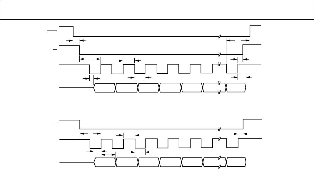
Figure 19 and Figure 20 show timing diagrams for interfacing to
the AD7705/AD7706, with
CS
used to decode the parts. Figure 19
shows a read operation from the AD7705/AD7706 output shift
register, and
Figure 20 shows a write operation to the input shift
register. It is possible to read the same data twice from the
output register, even though the
DRDY
line returns high after
the first read operation. Care must be taken, however, to ensure
that the read operation is complete before the next output
update takes place.
The AD7705/AD7706 serial interface can operate in 3-wire
mode by tying the
CS
input low. In this case, the SCLK, DIN,
and DOUT lines are used to communicate with the AD7705/
AD7706, and the status of
DRDY
can be obtained by interrogating
the MSB of the communication register. This scheme is suitable
for interfacing to microcontrollers. If
CS
is required as a decoding
signal, it can be generated from a port bit. For microcontroller
interfaces, it is recommended that the SCLK idles high between
data transfers.
The AD7705/AD7706 can also be operated with
CS
used as a
frame synchronization signal. This scheme is suitable for DSP
interfaces. In this case, the first bit (MSB) is effectively clocked
out by
CS
, because
CS
normally occurs after the falling edge of
SCLK in DSP interfaces. The SCLK can continue to run between
data transfers, provided that the timing numbers are obeyed.
The serial interface can be reset by exercising the
RESET
input.
It can also be reset by writing a series of 1s on the DIN input. If
Logic 1 is written to the AD7705/AD7706 DIN line for at least
32 serial clock cycles, the serial interface is reset. This ensures
that in 3-wire systems, if the interface is lost via either a software
error or a glitch in the system, it can be reset to a known state.
This state returns the interface to where the AD7705/AD7706
are expecting a write operation to their communication registers.
This operation in itself does not reset the contents of any registers,
but it is advisable to set up all registers again, because the
information written to the registers is unknown due to the
interface being lost.
Some microprocessor or microcontroller serial interfaces have a
single serial data line. In this case, it is possible to connect the
AD7705/AD7706 DATA OUT and DATA IN lines together and
connect them to the single data line of the processor. A 10 kΩ
pull-up resistor should be used on this single data line. In this
case, if the interface is lost, the procedure to reset it back to a
known state is somewhat different than previously described
because the read and write operations share the same line. Instead,
a read operation of 24 serial clocks is required, followed by a write
operation where Logic 1 is written for at least 32 serial clock
cycles to ensure that the serial interface resets to a known state.