AD7705/AD7706
Rev. C | Page 16 of 44
ON-CHIP REGISTERS
The AD7705/AD7706 each contain eight on-chip registers that
can be accessed via the serial port. The first of these is a
communication register that controls the channel selection,
decides whether the next operation is a read or write operation,
and decides which register the next read or write operation
accesses.
All communication to the AD7705/AD7706 must start with a
write operation to the communication register. After a power-
on or reset, the device expects a write to its communication
register. The data written to this register determines whether
the next operation is a read or write operation and to which
register this operation occurs. Therefore, write access to any
register on the part starts with a write operation to the
communication register, followed by a write to the selected
register. Likewise, a read operation from any register on the
part, including the communication register itself and the output
data register, starts with a write operation to the communica-
tion register, followed by a read operation from the selected
register. The communication register also controls the standby
mode and channel selection. The
DRDY
status is available by
reading from the communication register.
The second register is a setup register that determines
calibration mode, gain setting, bipolar/unipolar operation, and
buffered mode. The third register is labeled the clock register
and contains the filter selection bits and clock control bits. The
fourth register is the data register from which the output data is
accessed. The final registers are the calibration registers, which
store channel calibration data. The registers are discussed in
more detail in the following sections.
COMMUNICATION REGISTER
(RS2, RS1, RS0 = 0, 0, 0)
The communication register is an 8-bit register from which data
can be read or to which data can be written. All communication
to the part must start with a write operation to its communica-
tion register. The data written to the communication register
determines whether the next operation is a read or write
operation and to which register this operation takes place. After
the read or write operation is complete, the interface returns to
its default state, where it expects a write operation to the
communication register. In situations where the interface
sequence is lost, a write operation of a least 32 serial clock
cycles with DIN high returns the ADC to its default state by
resetting the part.
Table 10 outlines the bit designations for the
communication register.
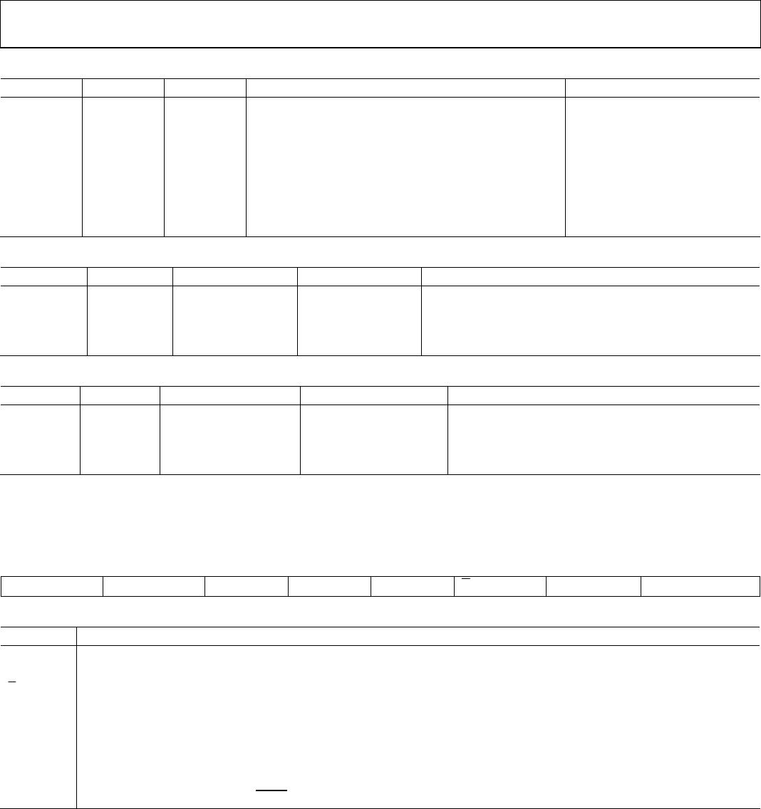
Table 9. Communication Register
0/
DRDY
(0) RS2 (0) RS1 (0) RS0 (0) R/
W
(0) STBY (0) CH1 (0) CH0 (0)
Table 10. Communication Register Bit Description
Register Description
0/DRDY For a write operation to the communications register, a 0 must be written to this bit. If a 1 is written to this bit, the part does
not clock subsequent bits into the register. It stays at this bit location until a 0 is written. Then, the next seven bits are loaded
into the communication register. For a read operation, this bit provides the status of the DRDY
flag, which is the same as the
DRDY output pin.
RS2–RS0
Register Selection Bits. These bits are used to select which of the AD7705/AD7706 registers are being accessed during the
serial interface communication.
R/W Read/WRITE Select. This bit selects whether the next operation is a read or write operation. A 0 indicates a write cycle for the
next operation to the selected register, and a 1 indicates a read operation from the selected register.
STBY
Standby. Writing 1 to this bit puts the part into standby or power-down mode. In this mode, the part consumes only 10 μA of
power supply current. The part retains its calibration coefficients and control word information when in standby. Writing 0 to
this bit places the parts in normal operating mode.
CH1, CH0
Channel Select. These two bits select a channel for conversion or for access to the calibration coefficients, as outlined in
Table 12. Following a calibration on a channel, three pairs of calibration registers store the calibration coefficients. Table 12
(for the AD7705) and
Table 13 (for the AD7706) show which channel combinations have independent calibration coefficients.
With CH1 at Logic 1 and CH0 at Logic 0, the AD7705 looks at the AIN1(−) input internally shorted to itself, while the AD7706 looks
at the COMMON input internally shorted to itself. This can be used as a test method to evaluate the noise performance of the
parts with no external noise sources. In this mode, the AIN1(−)/COMMON input should be connected to an external voltage
within the allowable common-mode range for the parts.