MAX V Device Handbook
May 2011
MV51003-1.2
Subscribe
© 2011 Altera Corporation. All rights reserved. ALTERA, ARRIA, CYCLONE, HARDCOPY, MAX, MEGACORE, NIOS, QUARTUS and STRATIX are Reg. U.S. Pat. & Tm. Off.
and/or trademarks of Altera Corporation in the U.S. and other countries. All other trademarks and service marks are the property of their respective holders as described at
www.altera.com/common/legal.html. Altera warrants performance of its semiconductor products to current specifications in accordance with Altera’s standard warranty, but
reserves the right to make changes to any products and services at any time without notice. Altera assumes no responsibility or liability arising out of the application or use of any
information, product, or service described herein except as expressly agreed to in writing by Altera. Altera customers are advised to obtain the latest version of device
specifications before relying on any published information and before placing orders for products or services.
3. DC and Switching Characteristics for
MAX V Devices
This chapter covers the electrical and switching characteristics for MAX
®
V devices.
Electrical characteristics include operating conditions and power consumptions. This
chapter also describes the timing model and specifications.
You must consider the recommended DC and switching conditions described in this
chapter to maintain the highest possible performance and reliability of the MAX V
devices.
This chapter contains the following sections:
■ “Operating Conditions” on page 3–1
■ “Power Consumption” on page 3–10
■ “Timing Model and Specifications” on page 3–10
Operating Conditions
Table 3–1 through Table 3–15 on page 3–9 list information about absolute maximum
ratings, recommended operating conditions, DC electrical characteristics, and other
specifications for MAX V devices.
Absolute Maximum Ratings
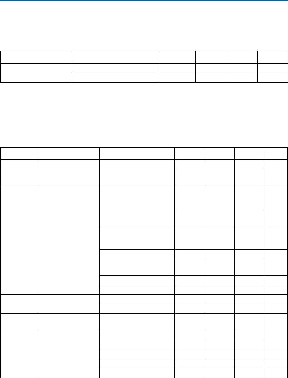
Table 3–1 lists the absolute maximum ratings for the MAX V device family.
Table 3–1. Absolute Maximum Ratings for MAX V Devices (Note 1), (2)
Symbol Parameter Conditions Minimum Maximum Unit
V
CCINT
Internal supply voltage With respect to ground –0.5 2.4 V
V
CCIO
I/O supply voltage — –0.5 4.6 V
V
I
DC input voltage — –0.5 4.6 V
I
OUT
DC output current, per pin — –25 25 mA
T
STG
Storage temperature No bias –65 150 °C
T
AMB
Ambient temperature Under bias (3) –65 135 °C
T
J
Junction temperature
TQFP and BGA packages
under bias
— 135 °C
Notes to Table 3–1:
(1) For more information, refer to the Operating Requirements for Altera Devices Data Sheet.
(2) Conditions beyond those listed in Table 3–1 may cause permanent damage to a device. Additionally, device operation at the absolute maximum
ratings for extended periods of time may have adverse affects on the device.
(3) For more information about “under bias” conditions, refer to Table 3–2.
May 2011
MV51003-1.2