3–22 Chapter 3: DC and Switching Characteristics for MAX V Devices
Timing Model and Specifications
MAX V Device Handbook May 2011 Altera Corporation
Table 330 lists the external I/O timing parameters for the F324 package of the
5M1270Z device.
Table 331 lists the external I/O timing parameters for the 5M2210Z device.
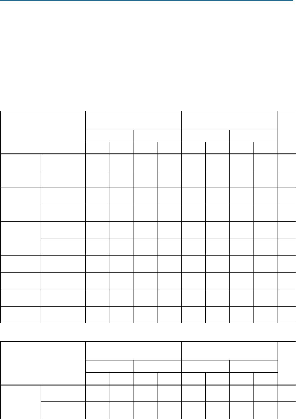
Table 3–30. Global Clock External I/O Timing Parameters for the 5M1270Z Device (Note 1), (2)
Symbol Parameter Condition
C4 C5, I5
Unit
Min Max Min Max
t
PD1
Worst case pin-to-pin delay through one LUT 10 pF 9.1 11.2 ns
t
PD2
Best case pin-to-pin delay through one LUT 10 pF 4.8 5.9 ns
t
SU
Global clock setup time 1.5 1.9 ns
t
H
Global clock hold time 0 0 ns
t
CO
Global clock to output delay 10 pF 2.0 6.0 2.0 7.4 ns
t
CH
Global clock high time 216 266 ps
t
CL
Global clock low time 216 266 ps
t
CNT
Minimum global clock period for 16-bit
counter
4.0 5.0 ns
f
CNT
Maximum global clock frequency for 16-bit
counter
247.5 201.1 MHz
Notes to Table 3–30:
(1) The maximum frequency is limited by the I/O standard on the clock input pin. The 16-bit counter critical delay performs faster than this global
clock input pin maximum frequency.
(2) Only applicable to the F324 package of the 5M1270Z device.
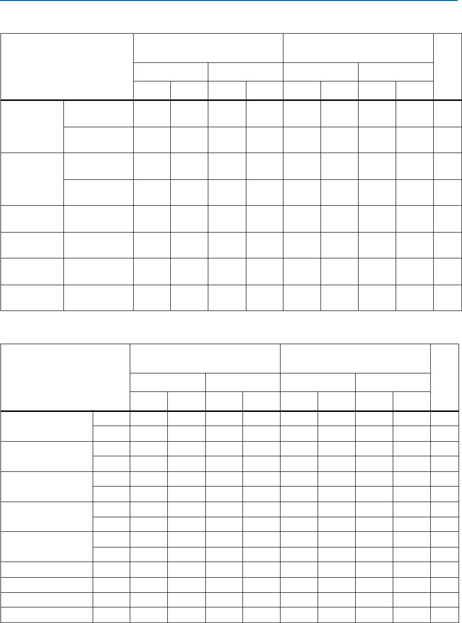
Table 3–31. Global Clock External I/O Timing Parameters for the 5M2210Z Device (Note 1)
Symbol Parameter Condition
C4 C5, I5
Unit
Min Max Min Max
t
PD1
Worst case pin-to-pin delay through one LUT 10 pF 9.1 11.2 ns
t
PD2
Best case pin-to-pin delay through one LUT 10 pF 4.8 5.9 ns
t
SU
Global clock setup time 1.5 1.9 ns
t
H
Global clock hold time 0 0 ns
t
CO
Global clock to output delay 10 pF 2.0 6.0 2.0 7.4 ns
t
CH
Global clock high time 216 266 ps
t
CL
Global clock low time 216 266 ps
t
CNT
Minimum global clock period for 16-bit
counter
4.0 5.0 ns
f
CNT
Maximum global clock frequency for 16-bit
counter
247.5 201.1 MHz
Note to Table 3–31:
(1) The maximum frequency is limited by the I/O standard on the clock input pin. The 16-bit counter critical delay performs faster than this global
clock input pin maximum frequency.
Chapter 3: DC and Switching Characteristics for MAX V Devices 3–23
Timing Model and Specifications
May 2011 Altera Corporation MAX V Device Handbook
External Timing I/O Delay Adders
The I/O delay timing parameters for the I/O standard input and output adders and
the input delays are specified by speed grade, independent of device density.
Table 332 through Table 3–36 on page 3–25 list the adder delays associated with I/O
pins for all packages. If you select an I/O standard other than 3.3-V LVTTL, add the
input delay adder to the external t
SU
timing parameters listed in Table 3–26 on
page 3–20 through Table 3–31. If you select an I/O standard other than 3.3-V LVTTL
with 16 mA drive strength and fast slew rate, add the output delay adder to the
external t
CO
and t
PD
listed in Table 3–26 on page 3–20 through Ta ble 3 –31.
Table 3–32. External Timing Input Delay Adders for MAX V Devices
I/O Standard
5M40Z/ 5M80Z/ 5M160Z/
5M240Z/ 5M570Z
5M1270Z/ 5M2210Z
Unit
C4 C5, I5 C4 C5, I5
Min Max Min Max Min Max Min Max
3.3-V LVTTL
Without Schmitt
Trigger
—0—0—0—0ps
With Schmitt
Trigger
387 442 480 591 ps
3.3-V LVCMOS
Without Schmitt
Trigger
—0—0—0—0ps
With Schmitt
Trigger
387 442 480 591 ps
2.5-V LVTTL /
LVCMOS
Without Schmitt
Trigger
42 42 246 303 ps
With Schmitt
Trigger
429 483 787 968 ps
1.8-V LVTTL /
LVCMOS
Without Schmitt
Trigger
378 368 695 855 ps
1.5-V LVCMOS
Without Schmitt
Trigger
681 658 1,334 1,642 ps
1.2-V LVCMOS
Without Schmitt
Trigger
1,055 1,010 2,324 2,860 ps
3.3-V PCI
Without Schmitt
Trigger
—0—0—0—0ps
Table 3–33. External Timing Input Delay t
GLOB
Adders for GCLK Pins for MAX V Devices (Part 1 of 2)
I/O Standard
5M40Z/ 5M80Z/ 5M160Z/
5M240Z/ 5M570Z
5M1270Z/ 5M2210Z
Unit
C4 C5, I5 C4 C5, I5
Min Max Min Max Min Max Min Max
3.3-V LVTTL
Without Schmitt
Trigger
—0—0—0—0ps
With Schmitt
Trigger
387 442 400 493 ps
3–24 Chapter 3: DC and Switching Characteristics for MAX V Devices
Timing Model and Specifications
MAX V Device Handbook May 2011 Altera Corporation
3.3-V LVCMOS
Without Schmitt
Trigger
—0—0—0—0ps
With Schmitt
Trigger
387 442 400 493 ps
2.5-V LVTTL /
LVCMOS
Without Schmitt
Trigger
242 242 287 353 ps
With Schmitt
Trigger
429 483 550 677 ps
1.8-V LVTTL /
LVCMOS
Without Schmitt
Trigger
378 368 459 565 ps
1.5-V LVCMOS
Without Schmitt
Trigger
681 658 1,111 1,368 ps
1.2-V LVCMOS
Without Schmitt
Trigger
1,055 1,010 2,067 2,544 ps
3.3-V PCI
Without Schmitt
Trigger
—0—0—7—9ps
Table 3–33. External Timing Input Delay t
GLOB
Adders for GCLK Pins for MAX V Devices (Part 2 of 2)
I/O Standard
5M40Z/ 5M80Z/ 5M160Z/
5M240Z/ 5M570Z
5M1270Z/ 5M2210Z
Unit
C4 C5, I5 C4 C5, I5
Min Max Min Max Min Max Min Max
Table 3–34. External Timing Output Delay and t
OD
Adders for Fast Slew Rate for MAX V Devices
I/O Standard
5M40Z/ 5M80Z/ 5M160Z/
5M240Z/ 5M570Z
5M1270Z/ 5M2210Z
Unit
C4 C5, I5 C4 C5, I5
Min Max Min Max Min Max Min Max
3.3-V LVTTL
16 mA—0—0—0—0ps
8 mA 39 58 84 104 ps
3.3-V LVCMOS
8 mA—0—0—0—0ps
4 mA 39 58 84 104 ps
2.5-V LVTTL / LVCMOS
14 mA 122 129 158 195 ps
7 mA 196 188 251 309 ps
1.8-V LVTTL / LVCMOS
6 mA 624 624 738 909 ps
3 mA 686 694 850 1,046 ps
1.5-V LVCMOS
4 mA 1,188 1,184 1,376 1,694 ps
2 mA 1,279 1,280 1,517 1,867 ps
1.2-V LVCMOS 3 mA 1,911 1,883 2,206 2,715 ps
3.3-V PCI 20 mA 39 58 4 5 ps
LVDS 122 129 158 195 ps
RSDS 122 129 158 195 ps

5M160ZM68I5N

Mfr. #:
Manufacturer:
Intel / Altera
Description:
CPLD - Complex Programmable Logic Devices CPLD - MAX V 128 Macro 52 IOs
Lifecycle:
New from this manufacturer.
Delivery:
DHL FedEx Ups TNT EMS
Payment:
T/T Paypal Visa MoneyGram Western Union