3–10 Chapter 3: DC and Switching Characteristics for MAX V Devices
Power Consumption
MAX V Device Handbook May 2011 Altera Corporation
Power Consumption
You can use the Altera
®
PowerPlay Early Power Estimator and PowerPlay Power
Analyzer to estimate the device power.
f For more information about these power analysis tools, refer to the PowerPlay Early
Power Estimator for Altera CPLDs User Guide and the PowerPlay Power Analysis chapter
in volume 3 of the Quartus II Handbook.
Timing Model and Specifications
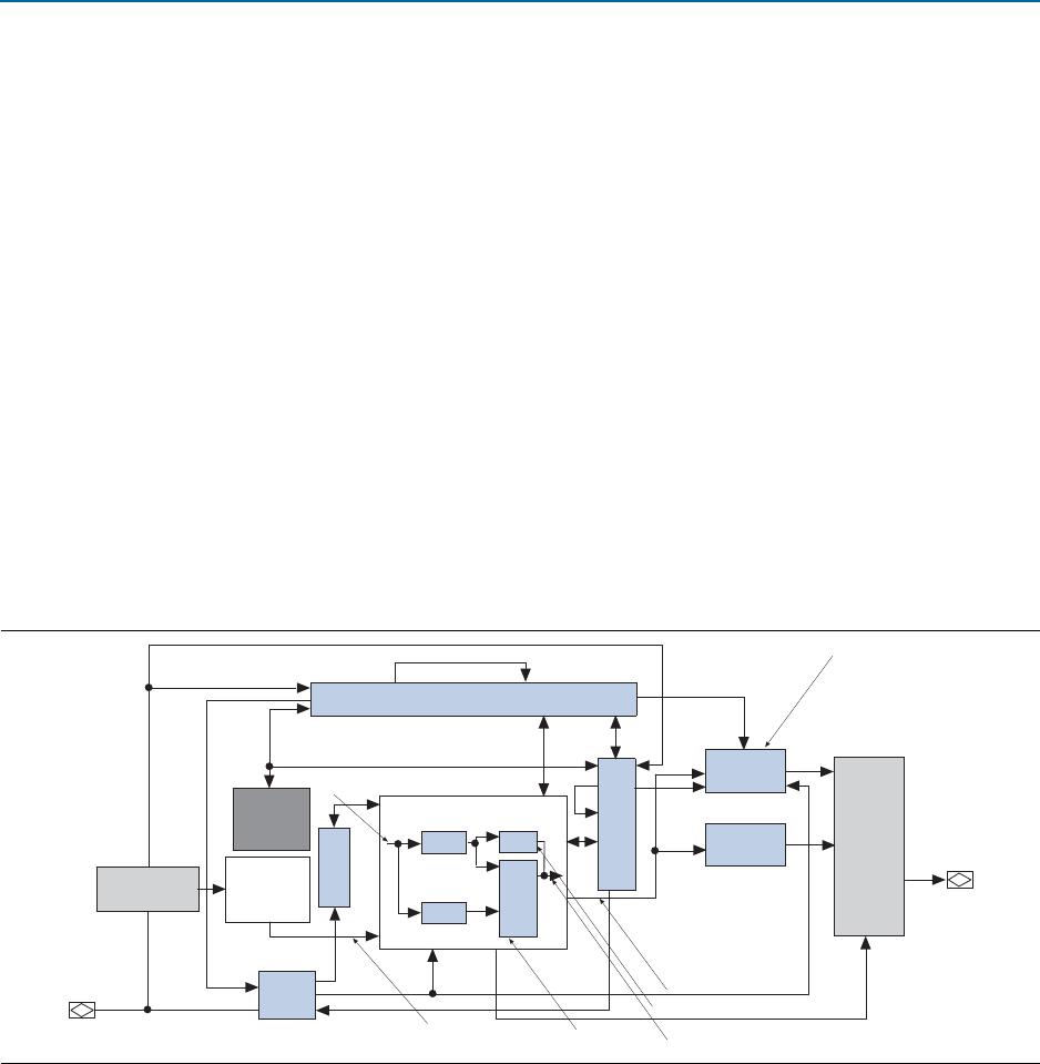
MAX V devices timing can be analyzed with the Altera Quartus
®
II software, a variety
of industry-standard EDA simulators and timing analyzers, or with the timing model
shown in Figure 3–2.
MAX V devices have predictable internal delays that allow you to determine the
worst-case timing of any design. The software provides timing simulation,
point-to-point delay prediction, and detailed timing analysis for device-wide
performance evaluation.
You can derive the timing characteristics of any signal path from the timing model
and parameters of a particular device. You can calculate external timing parameters,
which represent pin-to-pin timing delays, as the sum of the internal parameters.
f For more information, refer to AN629: Understanding Timing in Altera CPLDs.
Figure 3–2. Timing Model for MAX V Devices
I/O Pin
I/O Input Delay
t
IN
INPUT
Global Input Delay
t
C4
t
R4
Output
Delay
t
OD
t
XZ
t
ZX
t
LOCAL
t
GLOB
Logic Element
I/O Pin
t
FASTIO
Output Routing
Delay
User
Flash
Memory
From Adjacent LE
To Adjacent LE
Input Routing
Delay
t
DL
t
LUT
t
C
LUT Delay
Register Control
Delay
Register Delays
t
CO
t
SU
t
H
t
PRE
t
CLR
Data-In/LUT Chain
Data-Out
t
IODR
Output and Output Enable
Data Delay
t
IOE
t
COMB
Combinational Path Delay
Chapter 3: DC and Switching Characteristics for MAX V Devices 3–11
Timing Model and Specifications
May 2011 Altera Corporation MAX V Device Handbook
Preliminary and Final Timing
This section describes the performance, internal, external, and UFM timing
specifications. All specifications are representative of the worst-case supply voltage
and junction temperature conditions.
Timing models can have either preliminary or final status. The Quartus II software
issues an informational message during the design compilation if the timing models
are preliminary. Table 3–16 lists the status of the MAX V device timing models.
Preliminary status means the timing model is subject to change. Initially, timing
numbers are created using simulation results, process data, and other known
parameters. These tests are used to make the preliminary numbers as close to the
actual timing parameters as possible.
Final timing numbers are based on actual device operation and testing. These
numbers reflect the actual performance of the device under the worst-case voltage
and junction temperature conditions.
Performance
Table 317 lists the MAX V device performance for some common designs. All
performance values were obtained with the Quartus II software compilation of
megafunctions.
Table 3–16. Timing Model Status for MAX V Devices
Device Final
5M40Z v
5M80Z v
5M160Z v
5M240Z v
5M570Z v
5M1270Z v
5M2210Z v
Table 3–17. Device Performance for MAX V Devices (Part 1 of 2)
Resource
Used
Design Size and
Function
Resources Used
Performance
Unit
5M40Z/ 5M80Z/ 5M160Z/
5M240Z/ 5M570Z
5M1270Z/ 5M2210Z
Mode LEs
UFM
Blocks
C4 C5, I5 C4 C5, I5
LE
16-bit counter (1) 16 0 184.1 118.3 247.5 201.1 MHz
64-bit counter (1) 64 0 83.2 80.5 154.8 125.8 MHz
16-to-1 multiplexer 11 0 17.4 20.4 8.0 9.3 ns
32-to-1 multiplexer 24 0 12.5 25.3 9.0 11.4 ns
16-bit
XOR
function 5 0 9.0 16.1 6.6 8.2 ns
16-bit decoder with
single address line
5 0 9.2 16.1 6.6 8.2 ns
3–12 Chapter 3: DC and Switching Characteristics for MAX V Devices
Timing Model and Specifications
MAX V Device Handbook May 2011 Altera Corporation
Internal Timing Parameters
Internal timing parameters are specified on a speed grade basis independent of device
density. Table 3–18 through Table 3–25 on page 3–19 list the MAX V device internal
timing microparameters for LEs, input/output elements (IOEs), UFM blocks, and
MultiTrack interconnects.
f For more information about each internal timing microparameters symbol, refer to
AN629: Understanding Timing in Altera CPLDs.
UFM
512 × 16 None 3 1 10.0 10.0 10.0 10.0 MHz
512 × 16 SPI (2) 37 1 9.7 9.7 8.0 8.0 MHz
512 × 8
Parallel
(3)
73 1 (4) (4) (4) (4) MHz
512 × 16 I
2
C (3) 142 1 100 (5) 100 (5) 100 (5) 100 (5) kHz
Notes to Table 3–17:
(1) This design is a binary loadable up counter.
(2) This design is configured for read-only operation in Extended mode. Read and write ability increases the number of logic elements (LEs) used.
(3) This design is configured for read-only operation. Read and write ability increases the number of LEs used.
(4) This design is asynchronous.
(5) The I
2
C megafunction is verified in hardware up to 100-kHz serial clock line rate.
Table 3–17. Device Performance for MAX V Devices (Part 2 of 2)
Resource
Used
Design Size and
Function
Resources Used
Performance
Unit
5M40Z/ 5M80Z/ 5M160Z/
5M240Z/ 5M570Z
5M1270Z/ 5M2210Z
Mode LEs
UFM
Blocks
C4 C5, I5 C4 C5, I5
Table 3–18. LE Internal Timing Microparameters for MAX V Devices (Part 1 of 2)
Symbol Parameter
5M40Z/ 5M80Z/ 5M160Z/
5M240Z/ 5M570Z
5M1270Z/ 5M2210Z
Unit
C4 C5, I5 C4 C5, I5
Min Max Min Max Min Max Min Max
t
LUT
LE combinational look-up
table (LUT) delay
1,215 2,247 742 914 ps
t
COMB
Combinational path delay 243 309 192 236 ps
t
CLR
LE register clear delay 401 545 309 381 ps
t
PRE
LE register preset delay 401 545 309 381 ps
t
SU
LE register setup time
before clock
260 321 271 333 ps
t
H
LE register hold time
after clock
0 —0 —0 —0 ps
t
CO
LE register
clock-to-output delay
380 494 305 376 ps

5M160ZM68I5N

Mfr. #:
Manufacturer:
Intel / Altera
Description:
CPLD - Complex Programmable Logic Devices CPLD - MAX V 128 Macro 52 IOs
Lifecycle:
New from this manufacturer.
Delivery:
DHL FedEx Ups TNT EMS
Payment:
T/T Paypal Visa MoneyGram Western Union