Chapter 3: DC and Switching Characteristics for MAX V Devices 3–7
Operating Conditions
May 2011 Altera Corporation MAX V Device Handbook
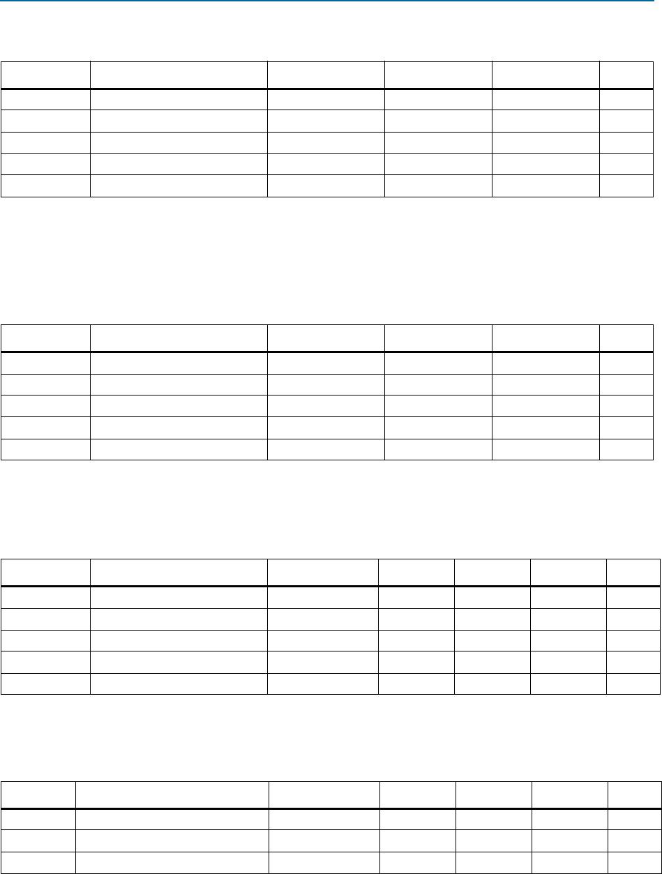
Table 3–9. 1.5-V I/O Specifications for MAX V Devices
Symbol Parameter Conditions Minimum Maximum Unit
V
CCIO
I/O supply voltage 1.425 1.575 V
V
IH
High-level input voltage 0.65 × V
CCIO
V
CCIO
+ 0.3 (2) V
V
IL
Low-level input voltage –0.3 0.35 × V
CCIO
V
V
OH
High-level output voltage IOH = –2 mA (1) 0.75 × V
CCIO
—V
V
OL
Low-level output voltage IOL = 2 mA (1) —0.25 × V
CCIO
V
Notes to Table 3–9:
(1) This specification is supported across all the programmable drive strength settings available for this I/O standard, as shown in the
MAX V Device Architecture chapter.
(2) This maximum V
IH
reflects the JEDEC specification. The MAX V input buffer can tolerate a V
IH
maximum of 4.0, as specified by the V
I
parameter
in Table 3–2 on page 3–2.
Table 3–10. 1.2-V I/O Specifications for MAX V Devices
Symbol Parameter Conditions Minimum Maximum Unit
V
CCIO
I/O supply voltage 1.14 1.26 V
V
IH
High-level input voltage 0.8 × V
CCIO
V
CCIO
+0.3 V
V
IL
Low-level input voltage –0.3 0.25 × V
CCIO
V
V
OH
High-level output voltage IOH = –2 mA (1) 0.75 × V
CCIO
—V
V
OL
Low-level output voltage IOL = 2 mA (1) —0.25×V
CCIO
V
Note to Table 3–10:
(1) This specification is supported across all the programmable drive strength settings available for this I/O standard, as shown in the
MAX V Device Architecture chapter.
Table 3–11. 3.3-V PCI Specifications for MAX V Devices (Note 1)
Symbol Parameter Conditions Minimum Typical Maximum Unit
V
CCIO
I/O supply voltage 3.0 3.3 3.6 V
V
IH
High-level input voltage 0.5 × V
CCIO
—V
CCIO
+ 0.5 V
V
IL
Low-level input voltage 0.5 0.3 × V
CCIO
V
V
OH
High-level output voltage IOH = –500 µA 0.9 × V
CCIO
——V
V
OL
Low-level output voltage IOL = 1.5 mA 0.1 × V
CCIO
V
Note to Table 3–11:
(1) 3.3-V PCI I/O standard is only supported in Bank 3 of the 5M1270Z and 5M2210Z devices.
Table 3–12. LVDS Specifications for MAX V Devices (Note 1)
Symbol Parameter Conditions Minimum Typical Maximum Unit
V
CCIO
I/O supply voltage 2.375 2.5 2.625 V
V
OD
Differential output voltage swing 247 600 mV
V
OS
Output offset voltage 1.125 1.25 1.375 V
Note to Table 3–12:
(1) Supports emulated LVDS output using a three-resistor network (LVDS_E_3R).
3–8 Chapter 3: DC and Switching Characteristics for MAX V Devices
Operating Conditions
MAX V Device Handbook May 2011 Altera Corporation
Bus Hold Specifications
Table 314 lists the bus hold specifications for the MAX V device family.
Table 3–13. RSDS Specifications for MAX V Devices (Note 1)
Symbol Parameter Conditions Minimum Typical Maximum Unit
V
CCIO
I/O supply voltage 2.375 2.5 2.625 V
V
OD
Differential output voltage swing 247 600 mV
V
OS
Output offset voltage 1.125 1.25 1.375 V
Note to Table 3–13:
(1) Supports emulated RSDS output using a three-resistor network (RSDS_E_3R).
Table 3–14. Bus Hold Specifications for MAX V Devices
Parameter Conditions
V
CCIO
Level
Unit1.2 V 1.5 V 1.8 V 2.5 V 3.3 V
Min Max Min Max Min Max Min Max Min Max
Low sustaining
current
V
IN
> V
IL
(maximum) 10 20 30 50 70 µA
High sustaining
current
V
IN
< V
IH
(minimum) –10 –20 –30 –50 –70 µA
Low overdrive
current
0 V < V
IN
< V
CCIO
—130—160—200—300—500µA
High overdrive
current
0 V < V
IN
< V
CCIO
–130 –160 –200 –300 –500 µA
Chapter 3: DC and Switching Characteristics for MAX V Devices 3–9
Operating Conditions
May 2011 Altera Corporation MAX V Device Handbook
Power-Up Timing
Table 315 lists the power-up timing characteristics for the MAX V device family.
Table 3–15. Power-Up Timing for MAX V Devices
Symbol Parameter Device Temperature Range Min Typ Max Unit
t
CONFIG
The amount of time from
when minimum V
CCINT
is
reached until the device
enters user mode (1)
5M40Z
Commercial and industrial 200 µs
Extended 300 µs
5M80Z
Commercial and industrial 200 µs
Extended 300 µs
5M160Z
Commercial and industrial 200 µs
Extended 300 µs
5M240Z (2)
Commercial and industrial 200 µs
Extended 300 µs
5M240Z (3)
Commercial and industrial 300 µs
Extended 400 µs
5M570Z
Commercial and industrial 300 µs
Extended 400 µs
5M1270Z (4)
Commercial and industrial 300 µs
Extended 400 µs
5M1270Z (5)
Commercial and industrial 450 µs
Extended 500 µs
5M2210Z
Commercial and industrial 450 µs
Extended 500 µs
Notes to Table 3–15:
(1) For more information about power-on reset (POR) trigger voltage, refer to the Hot Socketing and Power-On Reset in MAX V Devices chapter.
(2) Not applicable to the T144 package of the 5M240Z device.
(3) Only applicable to the T144 package of the 5M240Z device.
(4) Not applicable to the F324 package of the 5M1270Z device.
(5) Only applicable to the F324 package of the 5M1270Z device.

5M160ZM68I5N

Mfr. #:
Manufacturer:
Intel / Altera
Description:
CPLD - Complex Programmable Logic Devices CPLD - MAX V 128 Macro 52 IOs
Lifecycle:
New from this manufacturer.
Delivery:
DHL FedEx Ups TNT EMS
Payment:
T/T Paypal Visa MoneyGram Western Union