Chapter 3: DC and Switching Characteristics for MAX V Devices 3–25
Timing Model and Specifications
May 2011 Altera Corporation MAX V Device Handbook
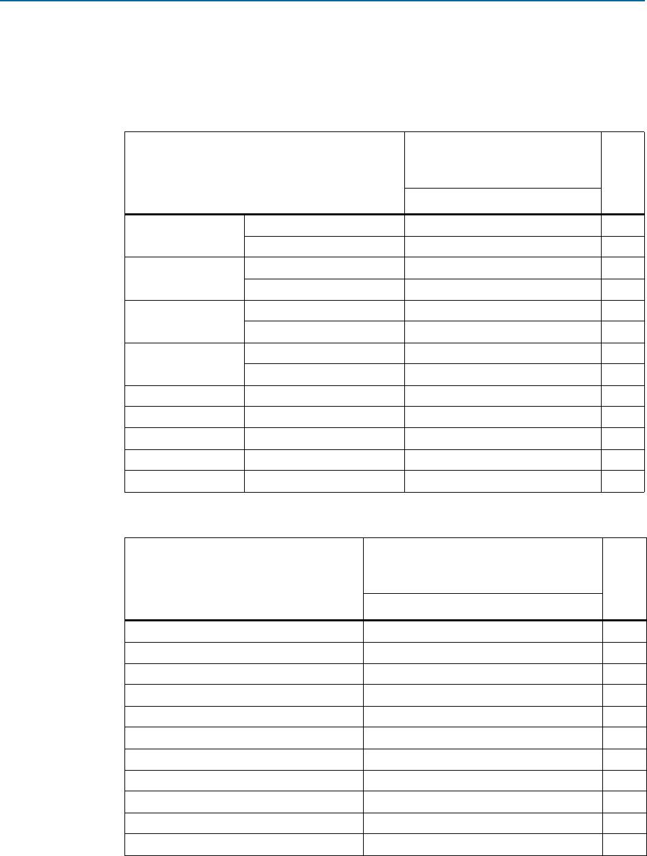
Table 3–35. External Timing Output Delay and t
OD
Adders for Slow Slew Rate for MAX V Devices
I/O Standard
5M40Z/ 5M80Z/ 5M160Z/
5M240Z/ 5M570Z
5M1270Z/ 5M2210Z
Unit
C4 C5, I5 C4 C5, I5
Min Max Min Max Min Max Min Max
3.3-V LVTTL
16 mA 5,913 6,043 6,612 6,293 ps
8 mA 6,488 6,645 7,313 6,994 ps
3.3-V LVCMOS
8 mA 5,913 6,043 6,612 6,293 ps
4 mA 6,488 6,645 7,313 6,994 ps
2.5-V LVTTL / LVCMOS
14 mA 9,088 9,222 10,021 9,702 ps
7 mA 9,808 9,962 10,881 10,562 ps
1.8-V LVTTL / LVCMOS
6 mA 21,758 21,782 21,134 20,815 ps
3 mA 23,028 23,032 22,399 22,080 ps
1.5-V LVCMOS
4 mA 39,068 39,032 34,499 34,180 ps
2 mA 40,578 40,542 36,281 35,962 ps
1.2-V LVCMOS 3 mA 69,332 70,257 55,796 55,477 ps
3.3-V PCI 20 mA 6,488 6,645 339 418 ps
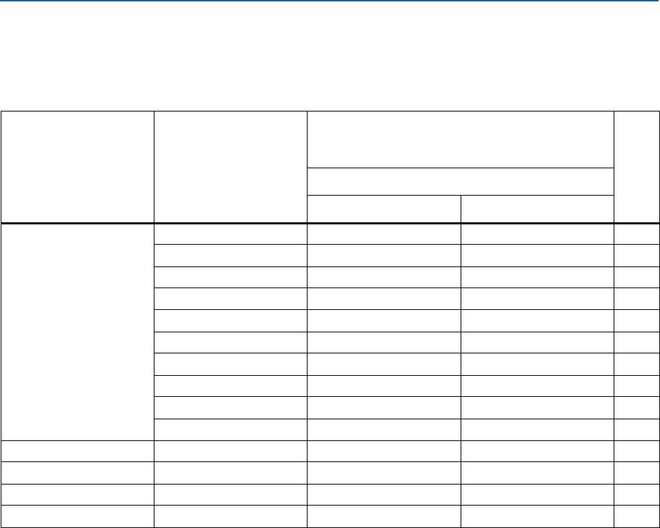
Table 3–36. IOE Programmable Delays for MAX V Devices
Parameter
5M40Z/ 5M80Z/ 5M160Z/
5M240Z/ 5M570Z
5M1270Z/ 5M2210Z
Unit
C4 C5, I5 C4 C5, I5
Min Max Min Max Min Max Min Max
Input Delay from Pin to Internal
Cells = 1
1,858 2,214 1,592 1,960 ps
Input Delay from Pin to Internal
Cells = 0
569 616 115 142 ps
3–26 Chapter 3: DC and Switching Characteristics for MAX V Devices
Timing Model and Specifications
MAX V Device Handbook May 2011 Altera Corporation
Maximum Input and Output Clock Rates
Tabl e 3 –3 7 and Table 3–38 list the maximum input and output clock rates for standard
I/O pins in MAX V devices.
Table 3–37. Maximum Input Clock Rate for I/Os for MAX V Devices
I/O Standard
5M40Z/ 5M80Z/ 5M160Z/
5M240Z/ 5M570Z/5M1270Z/
5M2210Z
Unit
C4, C5, I5
3.3-V LVTTL
Without Schmitt Trigger 304 MHz
With Schmitt Trigger 304 MHz
3.3-V LVCMOS
Without Schmitt Trigger 304 MHz
With Schmitt Trigger 304 MHz
2.5-V LVTTL
Without Schmitt Trigger 304 MHz
With Schmitt Trigger 304 MHz
2.5-V LVCMOS
Without Schmitt Trigger 304 MHz
With Schmitt Trigger 304 MHz
1.8-V LVTTL Without Schmitt Trigger 200 MHz
1.8-V LVCMOS Without Schmitt Trigger 200 MHz
1.5-V LVCMOS Without Schmitt Trigger 150 MHz
1.2-V LVCMOS Without Schmitt Trigger 120 MHz
3.3-V PCI Without Schmitt Trigger 304 MHz
Table 3–38. Maximum Output Clock Rate for I/Os for MAX V Devices
I/O Standard
5M40Z/ 5M80Z/ 5M160Z/
5M240Z/ 5M570Z/5M1270Z/
5M2210Z
Unit
C4, C5, I5
3.3-V LVTTL 304 MHz
3.3-V LVCMOS 304 MHz
2.5-V LVTTL 304 MHz
2.5-V LVCMOS 304 MHz
1.8-V LVTTL 200 MHz
1.8-V LVCMOS 200 MHz
1.5-V LVCMOS 150 MHz
1.2-V LVCMOS 120 MHz
3.3-V PCI 304 MHz
LVDS 304 MHz
RSDS 200 MHz
Chapter 3: DC and Switching Characteristics for MAX V Devices 3–27
Timing Model and Specifications
May 2011 Altera Corporation MAX V Device Handbook
LVDS and RSDS Output Timing Specifications
Tabl e 3 –3 9 lists the emulated LVDS output timing specifications for MAX V devices.
Table 3–39. Emulated LVDS Output Timing Specifications for MAX V Devices
Parameter Mode
5M40Z/ 5M80Z/ 5M160Z/
5M240Z/ 5M570Z/5M1270Z/
5M2210Z
Unit
C4, C5, I5
Min Max
Data rate (1), (2)
10 304 Mbps
9 304 Mbps
8 304 Mbps
7 304 Mbps
6 304 Mbps
5 304 Mbps
4 304 Mbps
3 304 Mbps
2 304 Mbps
1 304 Mbps
t
DUTY
—4555%
Total jitter (3) ——0.2UI
t
RISE
——450ps
t
FALL
——450ps
Notes to Table 3–39:
(1) The performance of the LVDS_E_3R transmitter system is limited by the lower of the two—the maximum data rate supported by LVDS_E_3R
I/O buffer or 2x (F
MAX
of the ALTLVDS_TX instance). The actual performance of your LVDS_E_3R transmitter system must be attained through
the Quartus II timing analysis of the complete design.
(2) For the input clock pin to achieve 304 Mbps, use I/O standard with V
CCIO
of 2.5 V and above.
(3) This specification is based on external clean clock source.

5M160ZM68I5N

Mfr. #:
Manufacturer:
Intel / Altera
Description:
CPLD - Complex Programmable Logic Devices CPLD - MAX V 128 Macro 52 IOs
Lifecycle:
New from this manufacturer.
Delivery:
DHL FedEx Ups TNT EMS
Payment:
T/T Paypal Visa MoneyGram Western Union