3–16 Chapter 3: DC and Switching Characteristics for MAX V Devices
Timing Model and Specifications
MAX V Device Handbook May 2011 Altera Corporation
1 The default slew rate setting for MAX V devices in the Quartus II design software is
“fast”.
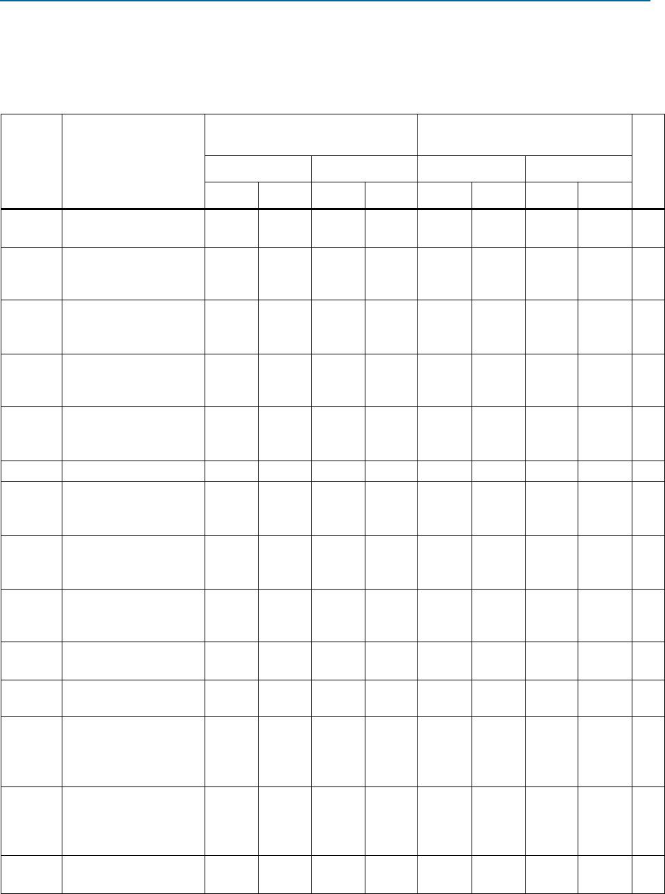
Table 3–24. UFM Block Internal Timing Microparameters for MAX V Devices (Part 1 of 2)
Symbol Parameter
5M40Z/ 5M80Z/ 5M160Z/
5M240Z/ 5M570Z
5M1270Z/ 5M2210Z
Unit
C4 C5, I5 C4 C5, I5
Min Max Min Max Min Max Min Max
t
ACLK
Address register clock
period
100 100 100 100 ns
t
ASU
Address register shift
signal setup to address
register clock
20—20—20—20—ns
t
AH
Address register shift
signal hold to address
register clock
20—20—20—20—ns
t
ADS
Address register data in
setup to address register
clock
20—20—20—20—ns
t
ADH
Address register data in
hold from address
register clock
20—20—20—20—ns
t
DCLK
Data register clock period 100 100 100 100 ns
t
DSS
Data register shift signal
setup to data register
clock
60—60—60—60—ns
t
DSH
Data register shift signal
hold from data register
clock
20—20—20—20—ns
t
DDS
Data register data in
setup to data register
clock
20—20—20—20—ns
t
DDH
Data register data in hold
from data register clock
20—20—20—20—ns
t
DP
Program signal to data
clock hold time
0—0—0—0ns
t
PB
Maximum delay between
program rising edge to
UFM
busy
signal rising
edge
960 960 960 960 ns
t
BP
Minimum delay allowed
from UFM
busy
signal
going low to program
signal going low
20—20—20—20—ns
t
PPMX
Maximum length of
busy
pulse during a program
100 100 100 100 µs
Chapter 3: DC and Switching Characteristics for MAX V Devices 3–17
Timing Model and Specifications
May 2011 Altera Corporation MAX V Device Handbook
t
AE
Minimum
erase
signal
to address clock hold
time
0—0—0—0ns
t
EB
Maximum delay between
the
erase
rising edge to
the UFM
busy
signal
rising edge
960 960 960 960 ns
t
BE
Minimum delay allowed
from the UFM
busy
signal going low to
erase
signal going low
20—20—20—20—ns
t
EPMX
Maximum length of
busy
pulse during an erase
500 500 500 500 ms
t
DCO
Delay from data register
clock to data register
output
—5—5—5—5ns
t
OE
Delay from
OSC_ENA
signal reaching UFM to
rising clock of
OSC
leaving the UFM
180 180 180 180 ns
t
RA
Maximum read access
time
—65—65—65—65ns
t
OSCS
Maximum delay between
the
OSC_ENA
rising edge
to the
erase/program
signal rising edge
250 250 250 250 ns
t
OSCH
Minimum delay allowed
from the
erase/program
signal
going low to
OSC_ENA
signal going low
250 250 250 250 ns
Table 3–24. UFM Block Internal Timing Microparameters for MAX V Devices (Part 2 of 2)
Symbol Parameter
5M40Z/ 5M80Z/ 5M160Z/
5M240Z/ 5M570Z
5M1270Z/ 5M2210Z
Unit
C4 C5, I5 C4 C5, I5
Min Max Min Max Min Max Min Max
3–18 Chapter 3: DC and Switching Characteristics for MAX V Devices
Timing Model and Specifications
MAX V Device Handbook May 2011 Altera Corporation
Figure 3–3 through Figure 3–5 show the read, program, and erase waveforms for
UFM block timing parameters listed in Table 3–24.
Figure 3–3. UFM Read Waveform
t
DCO
t
DCLK
t
DSS
t
DSH
t
ADH
t
ADS
t
ASU
t
ACLK
t
AH
ARShft
ARClk
ARDin
DRShft
DRClk
DRDin
DRDout
Program
Erase
Busy
16 Data Bits
9 Address Bits
OSC_ENA
Figure 3–4. UFM Program Waveform
t
ADS
t
ASU
t
ACLK
t
ADH
t
AH
t
DDS
t
DCLK
t
DSS
t
DSH
t
DDH
t
PB
t
BP
t
PPMX
t
OSCS
t
OSCH
ARShft
ARClk
ARDin
DRShft
DRClk
DRDin
DRDout
Program
Erase
Busy
16 Data Bits
9 Address Bits
OSC_ENA

5M160ZM68I5N

Mfr. #:
Manufacturer:
Intel / Altera
Description:
CPLD - Complex Programmable Logic Devices CPLD - MAX V 128 Macro 52 IOs
Lifecycle:
New from this manufacturer.
Delivery:
DHL FedEx Ups TNT EMS
Payment:
T/T Paypal Visa MoneyGram Western Union