LTC3300-1
10
33001fb
For more information www.linear.com/LTC3300-1
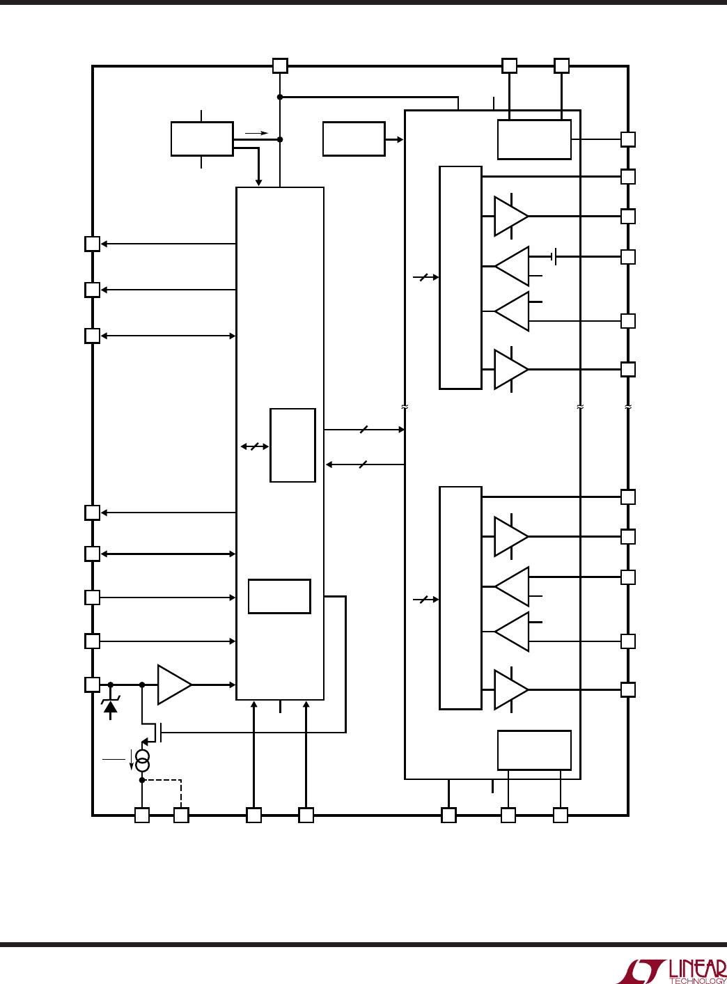
PIN FUNCTIONS
Note: The convention adopted in this data sheet is to refer
to the transformer winding paralleling an individual battery
cell as the primary and the transformer winding paralleling
multiple series-stacked cells as the secondary, regardless
of the direction of energy transfer.
G6S, G5S, G4S, G3S, G2S, G1S (Pins 1, 3, 5, 7, 9,
11): G1S through G6S are gate driver outputs for driving
external NMOS transistors connected in series with the
secondary windings of transformers whose primaries are
connected in parallel with battery cells 1 through 6. For
the minimum part count balancing application employing
a single transformer (CTRL = V
REG
), G2S through G6S
are no connects.
I6S, I5S, I4S, I3S, I2S, I1S (Pins 2, 4, 6, 8, 10, 12): I1S
through I6S are current sense inputs for measuring sec
-
ondary winding current in transformers whose primaries
are connected in parallel with battery cells 1 through 6.
For the minimum part count balancing application employ
-
ing
a single transformer (CTRL = V
REG
), I2S through I6S
should be tied to V
–
.
RTONS (Pin 13): Secondary Winding Max t
ON
Setting
Resistor. The RTONS pin servos to 1.2V. A resistor to V
–
programs the maximum on-time for all external NMOS
transistors connected in series with secondary windings.
This protects against a short-circuited current sense re
-
sistor in any secondary winding. To defeat this function,
connect R
TONS to V
REG
. The secondary winding OVP
threshold (see WDT pin) is also slaved to the value of the
R
TONS
resistor.
RTONP (Pin 14): Primary Winding Max t
ON
Setting
Resistor. The RTONP pin servos to 1.2V. A resistor to V
–
programs the maximum on-time for all external NMOS
transistors connected in series with primary windings.
This protects against a short-circuited current sense
resistor in any primary winding. To defeat this function,
connect RTONP to V
REG
.
CTRL: (Pin 15): Control Input. The CTRL pin configures
the LTC3300-1 for the minimum part count application
employing a single transformer if CTRL is tied to V
REG
or
for the multiple transformer application if CTRL is tied to
V
–
. This pin must be tied to either V
REG
or V
–
.
CSBI (Pin 16): Chip Select (Active Low) Input. The CSBI
pin interfaces to a rail-to-rail output logic gate if V
MODE
is tied to V
REG
. CSBI must be driven by the CSBO pin of
another LTC3300-1 if V
MODE
is tied to V
–
. See Serial Port
in the Applications Information section.
SCKI (Pin 17): Serial Clock Input. The SCKI pin interfaces
to a rail-to-rail output logic gate if V
MODE
is tied to V
REG
.
SCKI must be driven by the SCKO pin of another LTC3300-1
if V
MODE
is tied to V
–
. See Serial Port in the Applications
Information section.
SDI (Pin 18): Serial Data Input. When writing data to the
LTC3300-1, the SDI pin interfaces to a rail-to-rail output
logic gate if V
MODE
is tied to V
REG
or must be driven by
the SDOI pin of another LTC3300-1 if V
MODE
is tied to V
–
.
See Serial Port in the Applications Information section.
SDO (Pin 19): Serial Data Output. When reading data
from the LTC3300-1, the SDO pin is an NMOS open-drain
output if V
MODE
is tied to V
REG
. The SDO pin is not used
if V
MODE
is tied to V
–
. See Serial Port in the Applications
Information section.
WDT (Pin 20): Watchdog Timer Output (Active High). At
initial power-up and when not attempting to execute a valid
balance command, the WDT pin is high impedance and will
be pulled high (internally clamped to ~5.6V) if an external
pull-up resistor is present. While balancing (or attempt
-
ing to balance but not able to due to voltage/temperature
faults) and during normal communication activity, the WDT
pin is pulled low by a precision current source slaved to
the R
TONS
resistor. However, if no valid command byte is
written for 1.5 seconds (typical), the WDT output will go
back high. When WDT is high, all balancers are off. The
watchdog timer function can be disabled by connecting
WDT to V
–
. The secondary winding OVP function can also
be implemented using this pin (See Operation section).
V
–
(Pin 21): Connect V
–
to the most negative potential in
the series of cells.
I1P, I2P, I3P, I4P, I5P, I6P (Pins 22, 25, 28, 31, 34, 37):
I1P through I6P are current sense inputs for measuring
primary winding current in transformers connected in
parallel with battery cells 1 through 6.