LTC3300-1
27
33001fb
For more information www.linear.com/LTC3300-1
OPERATION
pin must be pulled high (tied to V
REG
). The other devices
in the daisy chain must have this pin pulled low (tied to V
–
)
to designate current mode communication. To designate
the top-of-stack device, the TOS pin on the top device of
a daisy chain must be tied high. The other devices in the
stack must have TOS tied low. See the application on the
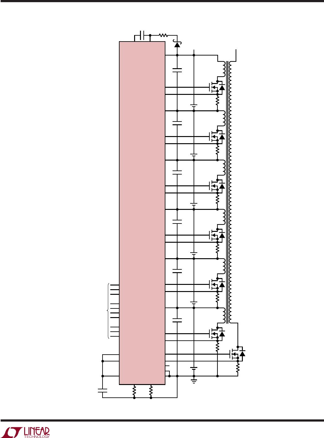
last page of this data sheet.
Command Byte
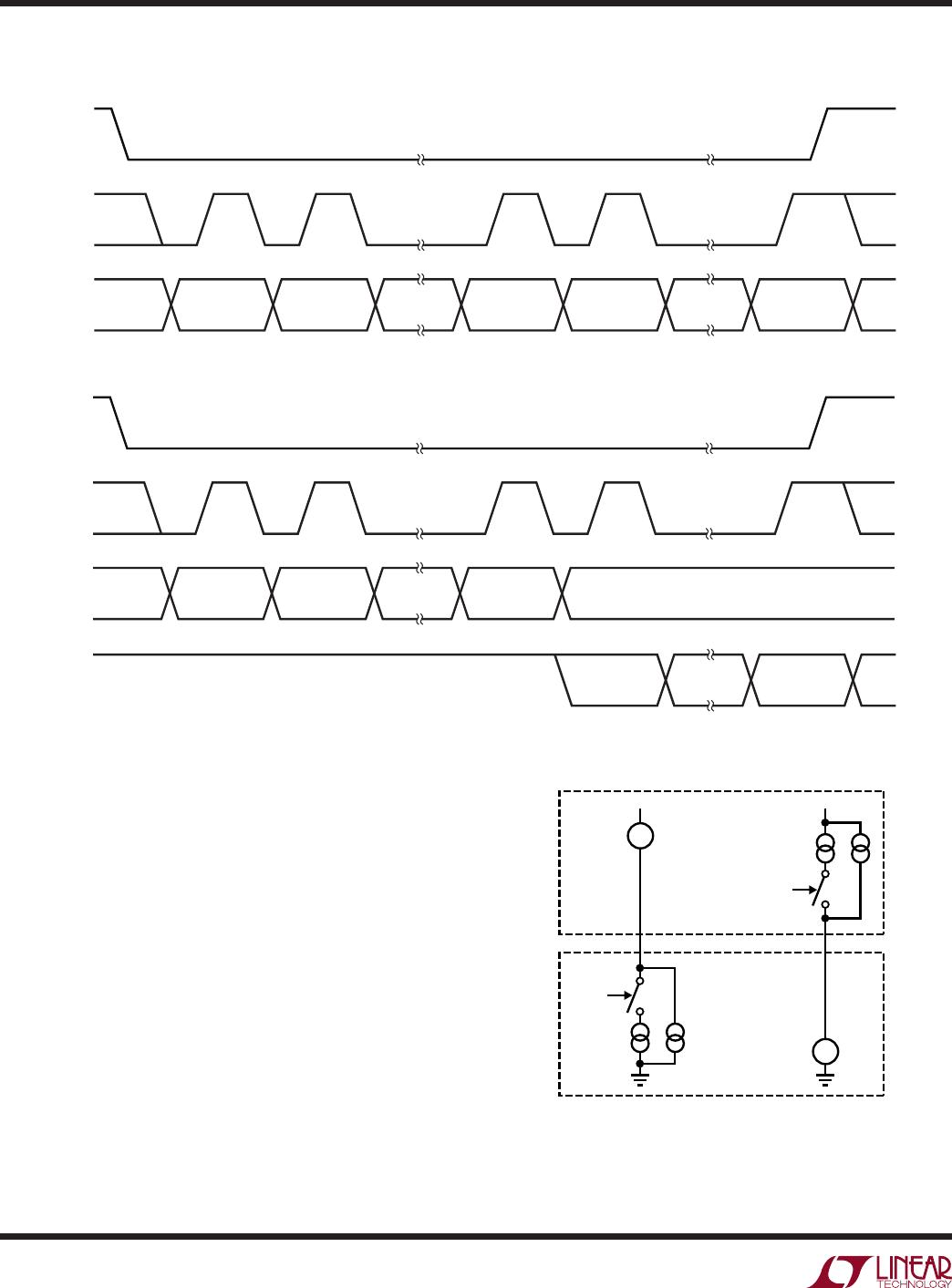
All communication to the LTC3300-1 takes place with CSBI
logic low. The first 8 clocked in data bits after a high-to-
low transition on CSBI represent the command byte and
are level-shifted through all LTC3300-1 ICs in the stack
so as to be simultaneously read by all LTC3300-1 ICs in
the stack. The 8-bit command byte is written MSB first
per Table 2. The first 5 bits must match a fixed internal
address [10101] which is common to all LTC3300-1’s in
the stack, or all subsequent data will be ignored until CSBI
transitions high and then low again. The 6th and 7th bits
program one of four commands as shown in Table 3. The
8th bit in the command byte must be set such that the
entire 8-bit command byte has even parity. If the parity is
incorrect, the current balance command being executed
(from the last previously successful write) is terminated
immediately and all subsequent (write) data is ignored until
CSBI transitions high and then low again. Incorrect parity
takes this action whether or not the address matches. This
thereby provides a fast means to immediately terminate
balancing-in-progress by intentionally writing a command
byte with incorrect parity.
Table 2. Command Byte Bit Mapping
(Defaults to 0x00 in Reset State)
1
(MSB)
0 1 0 1 CMDA CMDB Parity Bit
(LSB)
Table 3. Command Bits
CMDA CMDB Communication Action
0 0 Write Balance Command (without Executing)
0 1 Readback Balance Command
1 0 Read Balance Status
1 1 Execute Balance Command
Write Balance Command
If the command bits program Write Balance Command,
all subsequent write data must be mod 16 bits (before
CSBI transitions high) or it will be ignored. The internal
command holding register will be cleared which can be
verified on readback. The current balance command being
executed (from the last previously successful write) will
continue, but all active balancing will be turned off if an
Execute Balance Command is subsequently written. Each
LTC3300-1 in the stack expects 16 bits of write data writ
-
ten MSB first per Table 4. Successive 16-bit write data is
shifted in starting with the highest LTC3300-1 in the stack
and proceeding down the stack. In this manner
, the first
16 bits will be the write data for the topmost LTC3300-1 in
the stack and will have shifted through all other LTC3300-1
ICs in the stack. The last 16 bits will be the write data for
the bottom-most LTC3300-1 in the stack.
Table 4. Write Balance Command Data Bit Mapping (Defaults to 0x000F in Reset State)
D1A
(MSB)
D1B D2A D2B D3A D3B D4A D4B D5A D5B D6A D6B CRC[3] CRC[2] CRC[1] CRC[0]
(LSB)


