LTC3300-1
17
33001fb
For more information www.linear.com/LTC3300-1
OPERATION
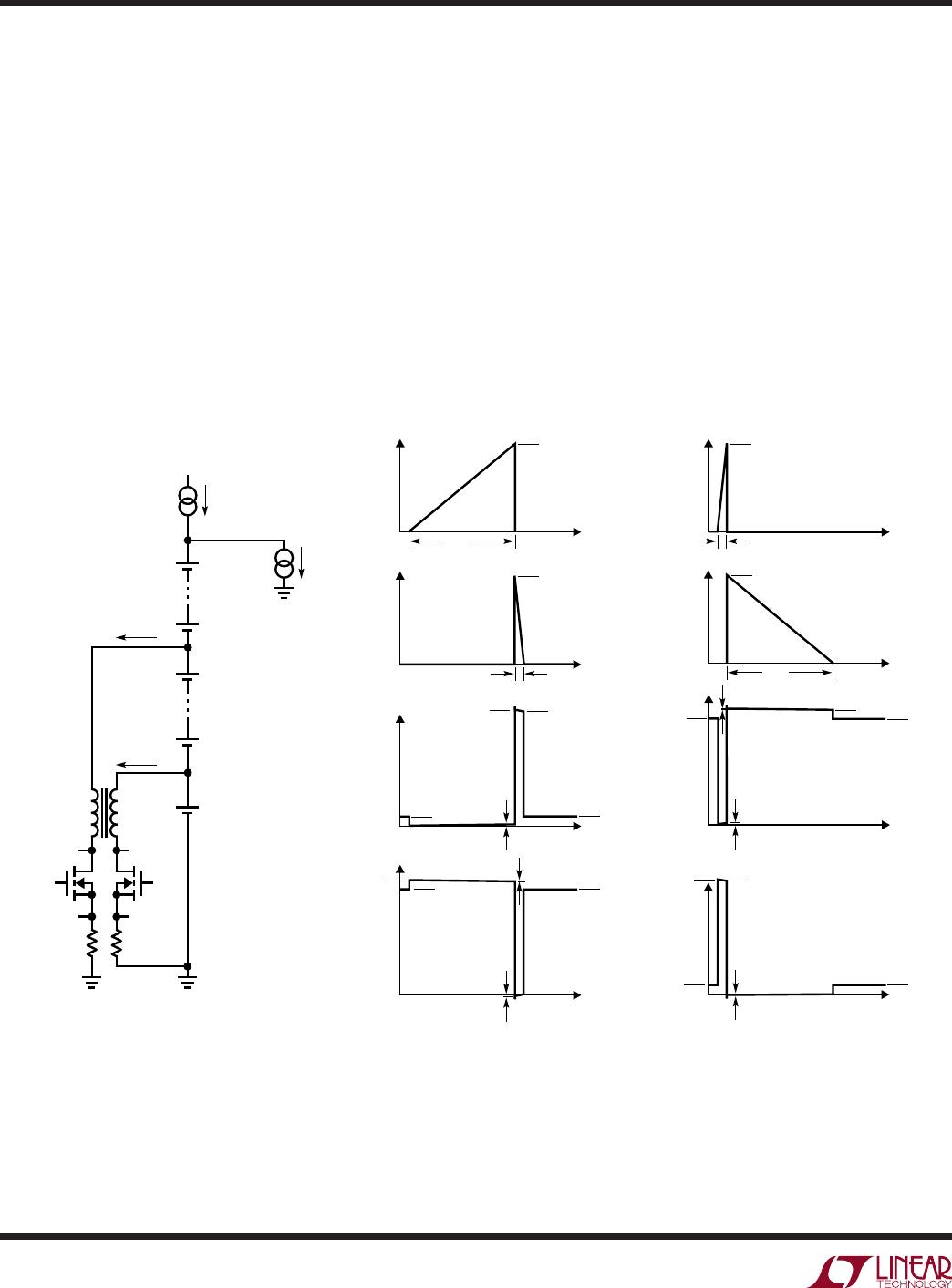
Cell Discharging (Synchronous)
When discharging is enabled for a given cell, the primary
side switch is turned on and current ramps in the primary
winding of the transformer until the programmed peak
current (I
PEAK_PRI
) is detected at the InP pin. The primary
side switch is then turned off, and the stored energy in
the transformer is transferred to the secondary-side cells
causing current to flow in the secondary winding of the
transformer. The secondary-side synchronous switch
is turned on to minimize power loss during the transfer
period until the secondary current drops to zero (detected
at In S). Once the secondary current reaches zero, the
secondary switch turns off and the primary-side switch
is turned back on thus repeating the cycle. In this manner,
charge is transferred from the cell being discharged to all
of the cells connected between the top and bottom of the
secondary side—thereby charging the adjacent cells. In the
example of Figure 2, the secondary-side connects across
12 cells including the cell being discharged.
I
PEAK_PRI
is programmed using the following equation:
I
PEAK _PRI
=
R
SNS_PRI
Cell discharge current (primary side) and secondary-side
charge recovery current are determined to first order by
the following equations:
I
DISCHARGE
=
PEAK _PRI
2
S
S+ T
⎛
⎝
⎜
⎞
⎠
⎟
I
SECONDARY
=
I
PEAK _PRI
2
1
S+ T
⎛
⎝
⎜
⎞
⎠
⎟
η
DISCHARG
where S is the number of secondary-side cells, 1:T is the
transformer turns ratio from primary to secondary, and
η
DISCHARGE
is the transfer efficiency from primary cell
discharge to the secondary side stack.
Cell Charging
When charging is enabled for a given cell, the secondary-
side switch for the enabled cell is turned on and current
flows from the secondary-side cells through the trans
-
former. Once I
PEAK_SEC
is reached in the secondary side
(detected at the In S pin), the secondary switch is turned
off and current then flows in the primary side thus charging
the selected cell from the entire stack of secondary cells. As
with the discharging case, the primary-side synchronous
switch is turned on to minimize power loss during the cell
charging phase. Once the primary current drops to zero,
the primary switch is turned off and the secondary-side
switch is turned back on thus repeating the cycle.
I
PEAK_SEC
is programmed using the following equation:
I
PEAK _SEC
=
R
SNS_SEC
Cell charge current and corresponding secondary-side
discharge current are determined to first order by the
following equations:
I
CHARGE
=
PEAK _SEC
2
S+ T
⎛
⎝
⎜
⎞
⎠
⎟
η
CHARGE
I
SECONDARY
=
I
PEAK _SEC
2
T
S+ T
⎛
⎝
⎜
⎞
⎠
⎟
where S is the number of secondary cells in the stack, 1:T
is the transformer turns ratio from primary to secondary,
and η
CHARGE
is the transfer efficiency from secondary-side
stack discharge to the primary-side cell.
Each balancer’s charge transfer “frequency” and duty
factor depend on a number of factors including I
PEAK_PRI
,
I
PEAK_SEC
, transformer winding inductances, turns ratio,
cell voltage and the number of secondary-side cells.
The frequency of switching seen at the gate driver outputs
is given by:
f
DISCHARGE
=
S+ T
•
CELL
L
PRI
•I
PEAK _PRI
f
CHARGE
=
S
S+ T
•
V
CELL
L
PRI
•I
PEAK _SEC
• T
where L
PRI
is the primary winding inductance.
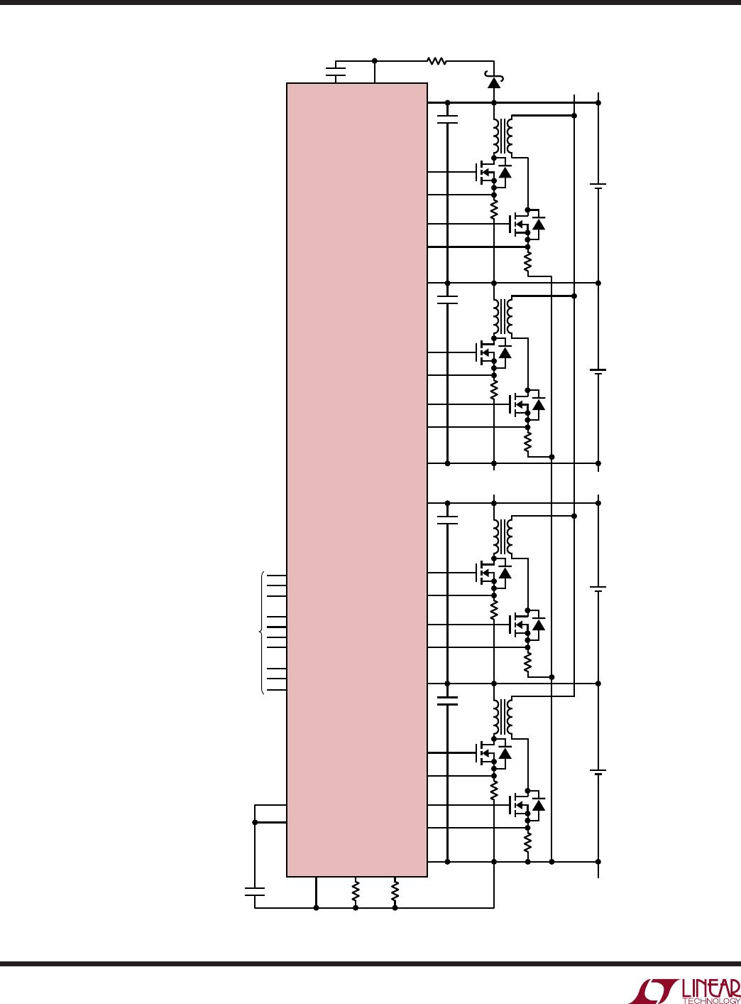
Figure 3 shows a fully populated LTC3300-1 application
employing all six balancers.