LTC3300-1
31
33001fb
For more information www.linear.com/LTC3300-1
APPLICATIONS INFORMATION
External FET Selection
In addition to being rated to handle the peak balancing
current, external NMOS transistors for both primary and
secondary windings must be rated with a drain-to-source
breakdown such that for the primary MOSFET:
V
DS(BREAKDOWN)|MIN
> V
CELL
+
V
STACK
+ V
DIODE
T
= V
CELL
1+
S
T
+
V
DIODE
T
and for the secondary MOSFET:
V
DS(BREAKDOWN)|MIN
>
V
STACK
+
T V
CELL
+
V
DIODE
( )
= V
CELL
S+ T
( )
+ T V
DIODE
where S is the number of cells in the secondary winding
stack and 1:T is the transformer turns ratio from primary
to secondary. For example, if there are 12 Li-Ion cells in
the secondary stack and using a turns ratio of 1:2, the
primary FETs would have to be rated for greater than 4.2V
(1 + 6) + 0.5 = 29.9V and the secondary FETs would have
to be rated for greater than 4.2V (12 + 2) + 2V = 60.8V.
Good design practice recommends increasing this voltage
rating by at least 20% to account for higher voltages present
due to leakage inductance ringing. See Table 7 for a list of
FETs that are recommended for use with the LTC3300-1.
Table 7
PART NUMBER MANUFACTURER I
DS(MAX)
V
DS(MAX)
SiR882DP Vishay 60A 100V
SiS892DN Vishay 25A 100V
IPD70N10S3-12 Infineon 70A 100V
IPB35N10S3L-26 Infineon 35A 100V
RJK1051DPB Renesas 60A 100V
RJK1054DPB Renesas 92A 100V
Transformer Selection
The LTC3300-1 is optimized to work with simple 2-wind-
ing transformers with a primary winding inductance of
between 1 and 20 microhenries, a 1:2 turns ratio (primar
y
to secondar
y), and the secondary winding paralleling up
to 12 cells. If a larger number of cells in the secondary
stack is desired for more efficient balancing, a transformer
with a higher turns ratio can be selected. For example, a
1:10 transformer would be optimized for up to 60 cells in
the secondary stack. In this case the external FETs would
need to be rated for a higher voltage (see above). In all
cases the saturation current of the transformer must be
selected to be higher than the peak currents seen in the
application.
See Table 8 for a list of transformers that are recommended
for use with the LTC3300-1.
Table 8
PART NUMBER MANUFACTURER
TURNS
RATIO*
PRIMARY
INDUCTANCE I
SAT
750312504 (SMT) Würth Electronics 1:1 3.5µH 10A
750312677 (THT) Würth Electronics 1:1 3.5µH 10A
MA5421-AL Coilcraft 1:1 3.4µH 10A
CTX02-18892-R Coiltronics 1:1 3.4µH 10A
XF0036-EP13S XFMRS Inc 1:1 3µH 10A
LOO-321 BH Electronics 1:1 3.4µH 10A
DHCP-X79-1001 TOKO 1:1 3.4µH 10A
C128057LF GCI 1:1 3.4µH 10A
T10857-1 Inter Tech 1:1 3.4µH 10A
*All transformers listed in the table are 8-pin components and can be
configured with turns ratios of 1:1, 1:2, 2:1, or 2:2.
Snubber Design
Careful attention must be paid to any transient ringing
seen at the drain voltages of the primary and secondary
winding FETs in application. The peak of the ringing should
not approach and must not exceed the breakdown voltage
rating of the FETs chosen. Minimizing leakage inductance
present in the application and utilizing good board layout
techniques can help mitigate the amount of ringing. In
some applications, it may be necessary to place a series
resistor + capacitor snubber network in parallel with each
winding of the transformer. This network will typically
lower efficiency by a few percent, but will keep the FETs
in a safer operating region. Determining values for R and
C usually requires some trial-and-error optimization in the
application. For the transformers shown in Table 8, good
starting point values for the snubber network are 330Ω
in series with 100pF.
LTC3300-1
32
33001fb
For more information www.linear.com/LTC3300-1
APPLICATIONS INFORMATION
Boosted Gate Drive Component Selection
(BOOST = V
REG
)
The external boost capacitor connected from BOOST
+
to
BOOST
supplies the gate drive voltage required for turning
on the external NMOS connected to G6P. This capacitor
is charged through the external Schottky diode from C6
to BOOST
+
when the NMOS is off (G6P = BOOST
= C5).
When the NMOS is to be turned on, the BOOST
driver
switches the lower plate of the capacitor from C5 to C6,
and the BOOST
+
voltage common modes up to one cell
voltage higher than C6. When the NMOS turns off again,
the BOOST
driver switches the lower plate of the capaci-
tor back to C5 so that the boost capacitor is refreshed.
A good rule of thumb is to make the value of the boost
capacitor 100
times that of the input capacitance of the
NMOS at G6P. For most applications, a 0.1µF/10V capacitor
will suffice.The reverse breakdown of the Schottky diode
must only be greater than 6V. To prevent an excessive and
potentially damaging surge current from flowing in the
boosted gate drive components during initial connection of
the battery voltages to the LTC3300-1, it is recommended
to place a 6.8Ω resistor in series with the Schottky diode
as shown in Figure 3. The surge current must be limited
to 1A to avoid potential damage.
Sizing the Cell Bypass Caps for Broken Connection
Protection
If a single connection to the battery stack is lost while bal
-
ancing, the differential cell voltages seen by the LTC3300-1
power circuit on each side of the break can increase or
decrease depending on whether charging or discharging
and where the actual break occurred. The worst-case
scenario is when the balancers on each side of the break
are both active and balancing in opposite directions. In
this scenario, the differential cell voltage will increase
rapidly on one side of the break and decrease rapidly
on the other. The cell overvoltage comparators working
in conjunction with appropriately-sized differential cell
bypass capacitors protect the LTC3300-1 and its associated
power components by shutting off all balancing before
any local differential cell voltage reaches its absolute
maximum rating. The comparator threshold (rising) is 5V,
and it takes 3µs to 6μs for the balancing to stop, during
which the bypass capacitor must prevent the differential
cell voltage
from increasing past 6V. Therefore, the mini
-
mum differential bypass capacitor value for full broken
connection protection is:
C
BYPASS(MIN)
=
I
CHARGE
+I
DISCHARGE
( )
6µs
6V 5V
If I
CHARGE
and I
DISCHARGE
are set nominally equal, then
approximately 12µF of real capacitance per amp of balance
current is required.
Protection from a broken connection to a cluster of sec
-
ondary windings is provided local to each LTC3300-1 in
the stack by the secondary winding OVP function (via
WDT pin) described in the Operation section. However
,
because of the interleaving of the transformer windings
up the stack, it is possible for a remote LTC3300-1 to still
act on the cell voltage seen locally by another LTC3300-1
at the point of the break which has shut itself off. For this
reason, each cluster of secondary windings must have
a dedicated connection to the stack separate from the
individual cell connection that it connects to.
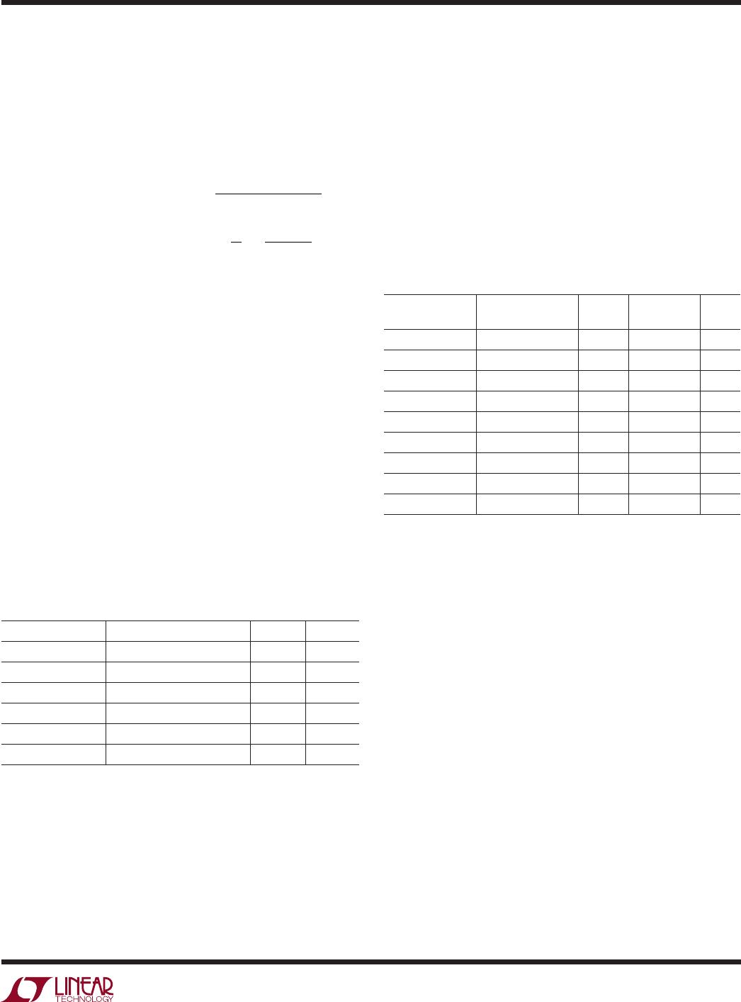
Using the LTC3300-1 with Fewer Than 6 Cells
To balance a series stack of N cells, the required number
of LTC3300-1 ICs is N/6 rounded up to the nearest integer.
Additionally, each LTC3300-1 in the stack must interface
to a minimum of 3 cells (must include C4, C5, and C6).
Thus, any stack of 3 or more cells can be balanced us
-
ing an appropriate stack of LTC3300-1 ICs. Unused cell
inputs (C1, C1 + C2, or C1 + C2 + C3) in a given LTC3300
-1 sub-stack should be shorted to V
(see Figure 11).
However, in all configurations, the write data remains at
16 bits. The LTC3300-1 will not act on the cell balancing
bits for the unused cell(s) but these bits are still included
in the CRC calculation.
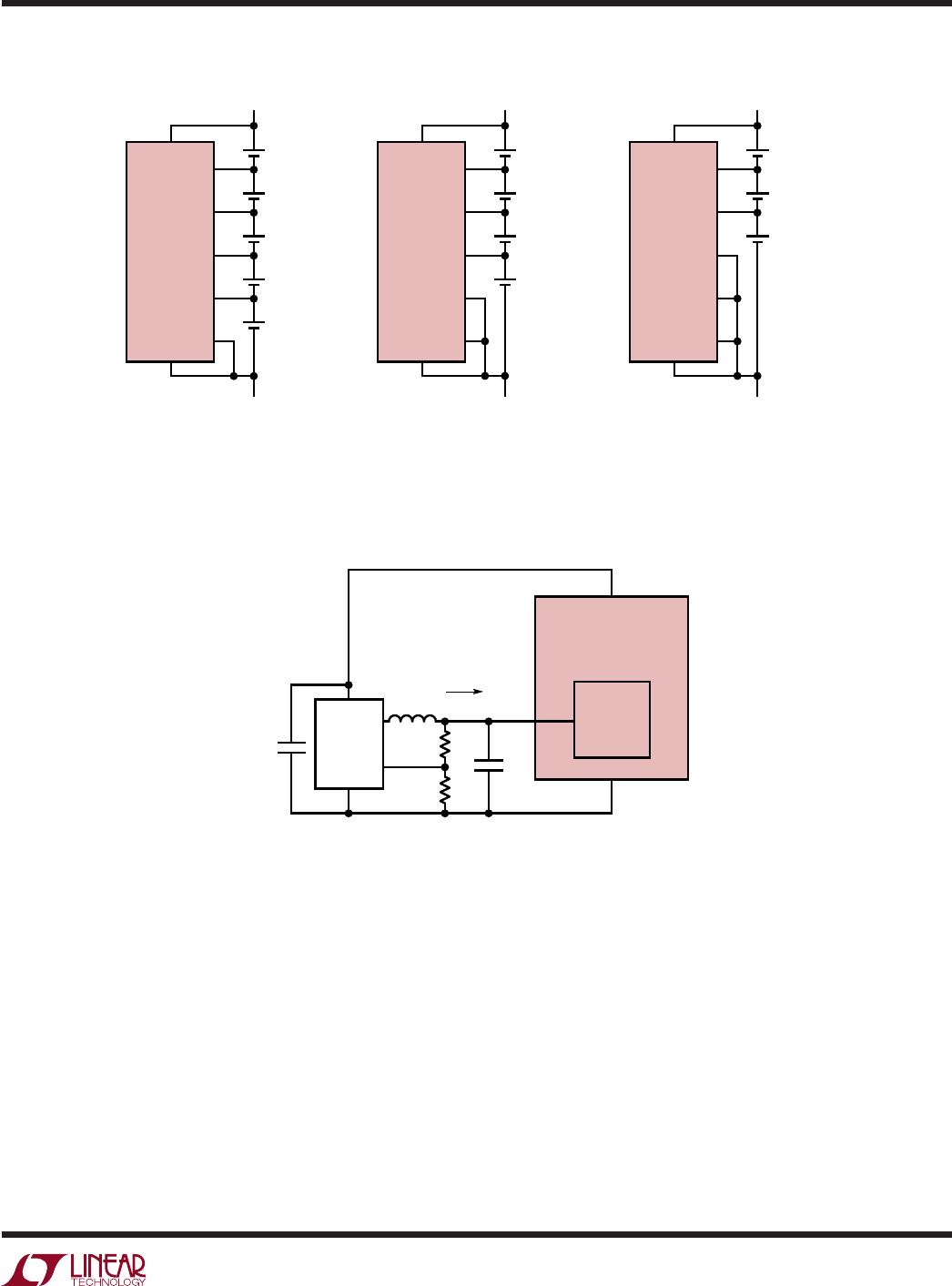
Supplementary Voltage Regulator Drive (>40mA)
The 4.8V linear voltage regulator internal to the LTC3300-1
is capable of providing 40mA at the V
REG
pin. If additional
current capability is required, the V
REG
pin can be back-
driven by an external low cost 5V buck DC/DC regulator
powered from C6 as shown in Figure 12. The internal
regulator of the LTC3300-1 has very limited sink current
capability and will not fight the higher forced voltage.
LTC3300-1
33
33001fb
For more information www.linear.com/LTC3300-1
APPLICATIONS INFORMATION
Figure 12. Adding External Buck DC/DC for >40mA V
REG
Drive
4.8V
LINEAR
VOLTAGE
REGULATOR
V
REG
C
OUT
R
FB2
V
LTC3300-1
C6
5V
I
OUT
> 40mA
L
R
FB1
C
IN
33001 F12
SW
GND
V
IN
BUCK
DC/DC
FB
Figure 11. Battery Stack Connections For 5, 4 or 3 Cells
+
CELL n + 4
+
CELL n + 3
+
CELL n + 2
+
CELL n + 1
+
CELL n
C6
LTC3300-1
(11a) Sub-Stack Using Only 5 Cells (11b) Sub-Stack Using Only 4 Cells (11c) Sub-Stack Using Only 3 Cells
V
C5
C4
C3
C2
C1
+
+
CELL n + 3
+
CELL n + 2
+
CELL n + 1
CELL n
C6
LTC3300-1
V
C5
C4
C3
C2
C1
+
+
+
CELL n + 2
CELL n + 1
CELL n
33001 F11
C6
LTC3300-1
V
C5
C4
C3
C2
C1

LTC3300IUK-1#PBF

Mfr. #:
Manufacturer:
Analog Devices / Linear Technology
Description:
Battery Management Hi Eff Bi-dir Multicell Bat Balancer
Lifecycle:
New from this manufacturer.
Delivery:
DHL FedEx Ups TNT EMS
Payment:
T/T Paypal Visa MoneyGram Western Union