LTC3300-1
37
33001fb
For more information www.linear.com/LTC3300-1
APPLICATIONS INFORMATION
Figure 15. Stack Terminal Currents in Shutdown
+
+
16µA
V
C6
LTC3300-1
7.5µA
16µA
V
C6
LTC3300-1
7.5µA
16µA
V
33001 F15
C6
LTC3300-1
7.5µA
16µA
3
V
CELL N – 6
C6CELL N
LTC3300-1
TOP OF STACK
BOTTOM OF STACK
23.5µA
TOS = 1
+
+
CELL N – 12
CELL N – 7
7.5µA
7.5µA
23.5µA
0µA
0µA
+
+
+
CELL 7
CELL 6
CELL 12
+
CELL 1
3
3
3
ALL
ZERO
C5
C4
C3
C2
C1
ALL
ZERO
C5
C4
C3
C2
C1
ALL
ZERO
C5
C4
C3
C2
C1
ALL
ZERO
C5
C4
C3
C2
C1
Analysis of Stack Terminal Currents in Shutdown
As given in the Electrical Characteristics table, the qui-
escent current of the LTC3300-1 when not balancing is
16μA
at the C6
pin and zero at the C1 through C5 pins.
All of this 16μA shows up at the V
pin of the LTC3300-1.
In addition, the SPI port when not communicating (i.e.,
CSBI = 1) contributes an additional 2.5μA per high side
line (CSBO/SCKO/SDOI), or 7.5μA to the V
pin current
of each LTC3300-1 in the stack which is not top of stack
(TOS = 0). This additional current does not add to the local
C6 pin current but rather to the C6 pin current of the next
higher LTC3300-1 in the stack as it is passed in through
the CSBI/SCKI/SDI pins. To the extent that the 16μA and
7.5μA currents match perfectly chip-to-chip in a long series
stack, the resultant stack terminal currents in shutdown
are as follows: 23.5μA out of the top of stack node, 7.5μA
out of the node 6 cells below top of stack, 7.5μA into the
node 6 cells above bottom of stack, and 23.5μA into the
bottom of stack node. All other intermediate node cur
-
rents are zero. This is shown graphically in Figure 15. For
the specific case of a 12-cell stack, this reduces to only
23.5µA out of the top of stack node and 23.5µA into the
bottom of stack node.
LTC3300-1
38
33001fb
For more information www.linear.com/LTC3300-1
How to Calculate the CRC
One simple method of computing an n-bit CRC is to perform
arithmetic modulo-2 division of the n+1 bit characteristic
polynomial into the m bit message appended with n ze
-
ros (m+n bits). Arithmetic modulo-2 division resembles
normal long division absent borrows and carries. At each
intermediate step of the long division, if the leading bit
of the
dividend is a 1, a 1 is entered in the quotient and
the dividend is exclusive-ORed bitwise with the divisor. If
the leading bit of the dividend is a 0, a 0 is entered in the
quotient and the dividend is exclusive-ORed bitwise with
n zeros. This process is repeated m times. At the end of
the long division, the quotient is disregarded and the n-
bit remainder is the CRC. This will be more clear in the
example to follow.
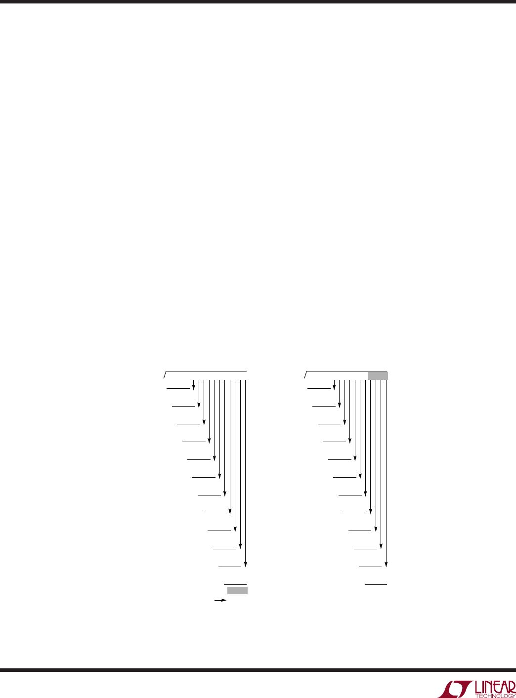
For the CRC implementation in the LTC3300-1, n = 4 and
m = 12. The characteristic polynomial employed is x
4
+ x
+ 1, which is shorthand for 1x
4
+ 0x
3
+ 0x
2
+ 1x
1
+ 1x
0
,
resulting in 10011 for the divisor. The message is the first
12 bits of the balance command. Suppose for example the
APPLICATIONS INFORMATION
desired balance command calls for simultaneous charging
of Cell 1 and synchronous discharging of Cell4. The 12-bit
message (MSB first) will be 110000010000. Appending
4 zeros results in 1100000100000000 for the dividend.
The long division is shown in Figure 16a with a resultant
CRC of 1101. Note that the CRC bits in the write balance
command are inverted. Thus the correct 16-bit balance
command is 1100000100000010. Figure16b shows the
same long division procedure being used to check the
CRC of data (command or status) read back from the
LTC3300-1. In this scenario, the remainder after the long
division must be zero (0000) for the data to be valid. Note
that the readback CRC bits must be inverted in the dividend
before performing the division.
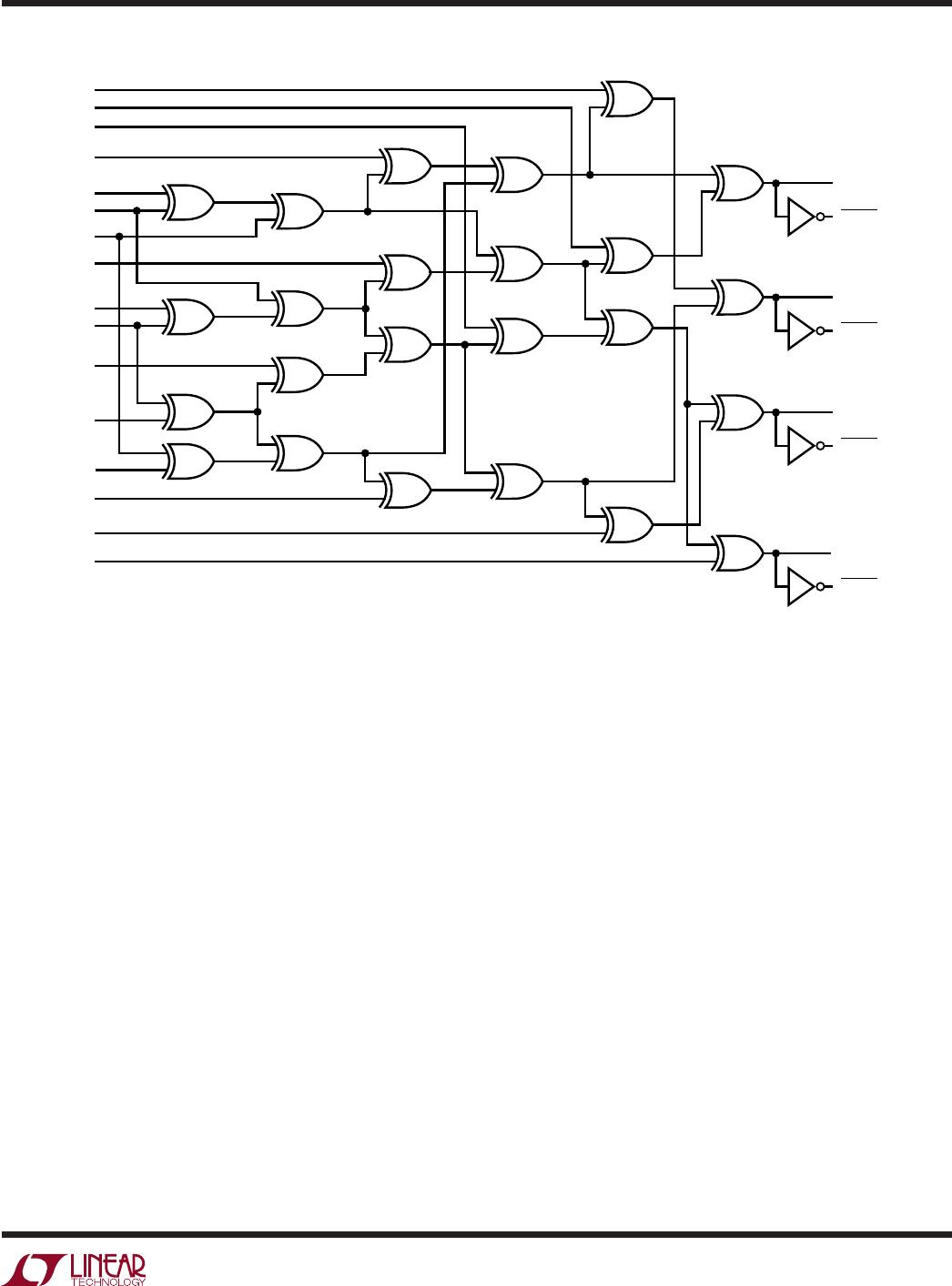
An alternate method to calculate the CRC is shown in
Figure 17 in which the balance command bits are input to
a combinational logic circuit comprised solely of 2-input
exclusive-OR gates. This “brute force” implementation is
easily replicated in a few lines of C code.
Figure 16. (a) Long Division Example to Calculate CRC for
Writes. (b) Long Division Example to Check CRC for Reads
1 1 0 1 0 1 1 0 1 0 1 1
1 0 0 1 1 1 1 0 0 0 0 0 1 0 0 0 0 0 0 0 0
1 0 0 1 1
1 0 1 1 0
1 0 0 1 1
0 1 0 1 0
0 0 0 0 0
1 0 1 0 1
1 0 0 1 1
0 1 1 0 0
0 0 0 0 0
1 1 0 0 0
1 0 0 1 1
1 0 1 1 0
1 0 0 1 1
0 1 0 1 0
0 0 0 0 0
1 0 1 0 0
1 0 0 1 1
0 1 1 1 0
0 0 0 0 0
1 1 1 0 0
1 0 0 1 1
1 1 1 1 0
1 0 0 1 1
REMAINDER = 1 1 0 1 = 4-BIT CRC
1 1 0 1 0 1 1 0 1 0 1 1
1 0 0 1 1 1 1 0 0 0 0 0 1 0 0 0 0 1 1 0 1
1 0 0 1 1
1 0 1 1 0
1 0 0 1 1
0 1 0 1 0
0 0 0 0 0
1 0 1 0 1
1 0 0 1 1
0 1 1 0 0
0 0 0 0 0
1 1 0 0 0
1 0 0 1 1
1 0 1 1 0
1 0 0 1 1
0 1 0 1 0
0 0 0 0 0
1 0 1 0 1
1 0 0 1 1
0 1 1 0 1
0 0 0 0 0
1 1 0 1 0
1 0 0 1 1
1 0 0 1 1
1 0 0 1 1
REMAINDER = 0
33001 F16
0 0 1 0 = 4-BIT CRC INVERTED
READBACK = 1100000100000010
DIVIDEND = 1100000100001101
(b)(a)
LTC3300-1
39
33001fb
For more information www.linear.com/LTC3300-1
Serial Communication Using the LTC6803 and LTC6804
The LTC3300-1 is compatible with and convenient to
use with all LTC monitor chips, such as the LTC6803 and
LTC6804. Figure 20 in the Typical Applications section
shows the serial communications connections for a joint
LTC3300-1/LTC6803-1 BMS using a common micropro
-
cessor SPI port. The SCKI, SDI, and SDO lines of the
lowermost L
TC3300-1 and L
TC6803-1 are tied together. The
CSBI lines, however, must be separated to prevent talking
to both ICs at the same time. This is easily accomplished
by using one of the GPIO outputs from the LTC6803-1
to gate and invert the CSBI line to the LTC3300-1. In this
setup, communicating to the LTC6803-1 is no different
than without the LTC3300-1, as the GPIO1 output bit is
normally high. To talk to the LTC3300-1, written commands
must be “bookended” with a GPIO1 negation write to the
LTC6803-1 prior to talking to the LTC3300-1 and with
a GPIO1 assertion write after talking to the LTC3300-1.
Communication “up the stack” passes between LTC3300-1
ICs and between LTC6803-1 ICs as shown.
APPLICATIONS INFORMATION
Figure 17. Combinational Logic Circuit Implementation of The CRC Calculator
CRC [3]
CRC [3]
CRC [2]
CRC [1]
CRC [0]
33001 F17
D6B
“Ø”
“Ø”
“Ø”
“Ø”
D5B
D3B
D1B
D2A
D5A
D3A
D1A
D4B
D2B
D4A
D6A
CRC [2]
CRC [1]
CRC [0]
The Typical Application shown on the back page of this
data sheet shows the serial communication connections for
a joint LTC3300-1/LTC6804-1 BMS. Each stacked 12-cell
module contains two LTC3300-1 ICs and a single LTC6804-1
monitor IC. The upper LTC3300-1 in each module is con
-
figured with V
MODE
= 0, TOS = 1, and receives its serial
communication from the lower LTC3300-1 in the same
module, which itself is configured with V
MODE
= 1, TOS
= 0. The LTC6804-1 in the same module is configured to
provide an effective SPI port output at its GPIO3, GPIO4,
and GPIO5 pins which connect directly to the low side
communication pins (CSBI, SDI=SDO, SCKI) of the lower
LTC3300-1. Communication to the lowermost LTC6804-1
and between monitor chips is done via the LTC6820 and
the isoSPI™ interface. In this application, unused battery
cells can be shorted from the bottom of any module (i.e.,
outside the module, not on the module board) as shown
without any decrease in monitor accuracy.

LTC3300IUK-1#PBF

Mfr. #:
Manufacturer:
Analog Devices / Linear Technology
Description:
Battery Management Hi Eff Bi-dir Multicell Bat Balancer
Lifecycle:
New from this manufacturer.
Delivery:
DHL FedEx Ups TNT EMS
Payment:
T/T Paypal Visa MoneyGram Western Union