LTC3300-1
21
33001fb
For more information www.linear.com/LTC3300-1
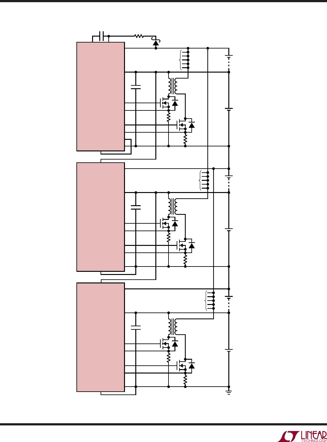
OPERATION
Gate Drivers/Gate Drive Comparators
All secondary-side gate drivers (G1S through G6S) are
powered from the V
REG
output, pulling up to 4.8V when
on and pulling down to V
–
when off. All primary-side
gate drivers (G1P through G6P) are powered from their
respective cell voltage and the next cell voltage higher in
the stack (see Table 1). An individual cell balancer will only
be enabled if its corresponding cell voltage is greater than
2V and the cell voltage of the next higher cell in the stack
is also greater than 2V. For the G6P gate driver output,
the next higher cell in the stack is C1 of the next higher
LTC3300-1 in the stack (if present) and is only used if the
boosted gate drive is disabled (by connecting BOOST =
V
–
). If the boosted gate drive is enabled (by connecting
BOOST = V
REG
), only the C6 cell voltage is looked at to
enable balancing of Cell 6. In the case of the topmost
LTC3300-1 in the stack, the boosted gate drive must be
enabled. The boosted gate drive requires an external diode
from C6 to BOOST
+
and a boost capacitor from BOOST
+
to
BOOST
–
. For information on selecting these components,
refer to the Applications Information section. Also note
that the dynamic supply current referred to in Note 4 of
the Electrical Characteristics table adds to the terminal
currents of the pins indicated in the Voltage When Off and
Voltage When On columns of Table 1.
The gate drive comparators have a DC hysteresis of 70mV.
For improved noise immunity, the inputs are internally
low pass filtered and the outputs are filtered so as to
not transition unless the internal comparator state is
unchanged for 3µs to 6µs (typical). If insufficient gate drive
is detected while active balancing is in progress (perhaps,
for example, if the stack is under heavy load), the affected
balancer(s) and only the affected balancer(s) will
shut off.
The balance command remains stored in memory, and
active balancing will resume where it left off if sufficient
gate drive is subsequently restored. This can happen if,
for example, the stack is being charged.
Cell Overvoltage Comparators
In addition to sufficient gate drive being required to enable
balancing, there are additional comparators which disable
all active balancing if any of the six individual cell voltages
is greater than 5V. These comparators have a DC hysteresis
of 500mV. For improved noise immunity, the inputs are
internally low pass filtered and the outputs are filtered so
as to not transition unless the internal comparator state
is unchanged for 3µs to 6µs (typical). If any cell voltage
goes overvoltage while active balancing is in progress,
all active balancers will shut off. The balance command
remains stored in memory, and active balancing will resume
where if left off if the cell voltage subsequently comes back
in range. These comparators will protect the LTC3300-1 if
a connection to a battery is lost while balancing and the
cell voltage is still increasing as a result of that balancing.
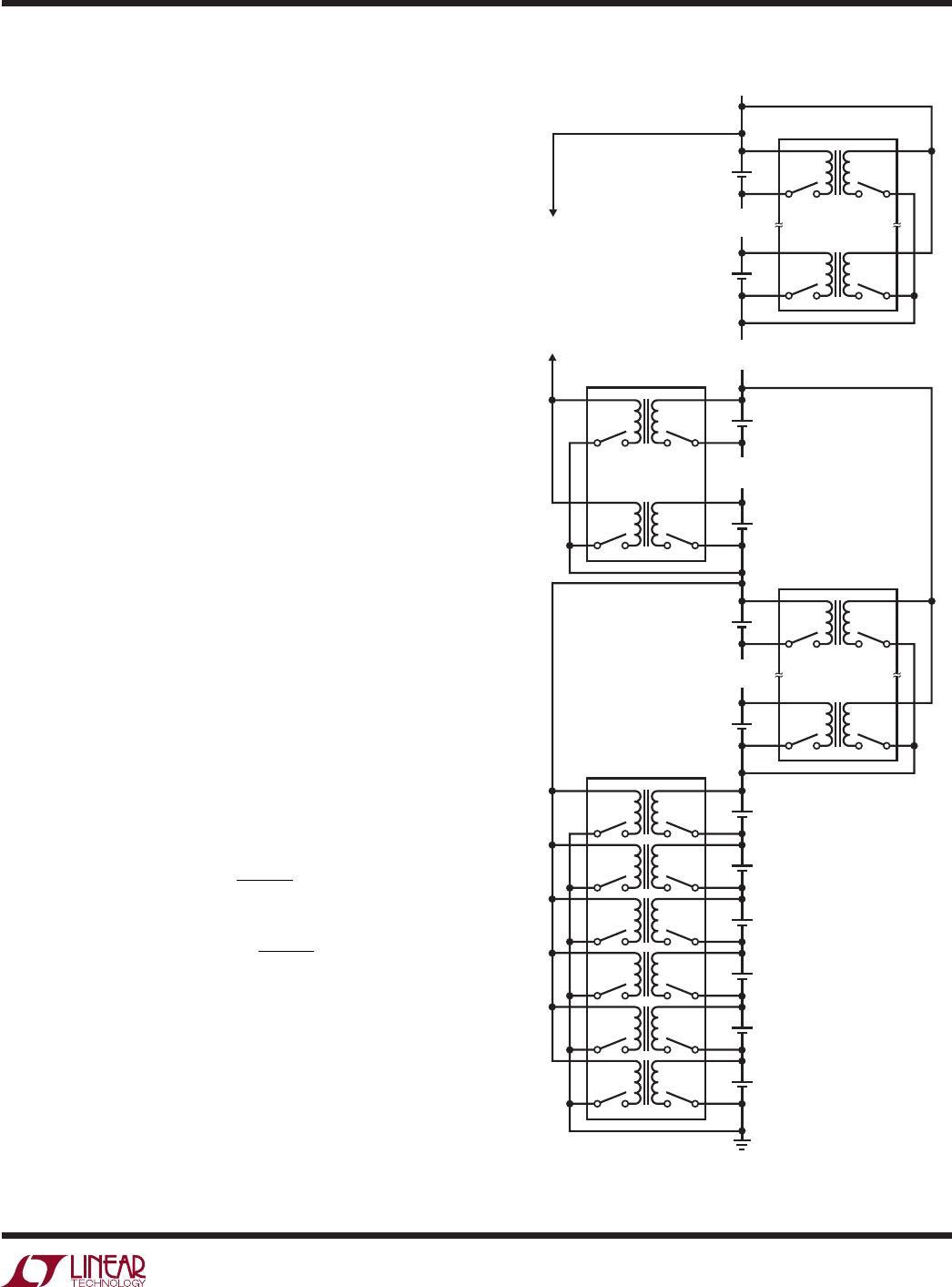
Table 1
DRIVER OUTPUT VOLTAGE WHEN OFF VOLTAGE WHEN ON GATE DRIVE REQUIRED TO ENABLE BALANCING
G1P V- C2 (C2 – C1) ≥ 2V and (C1 – V
–
) ≥2V
G2P C1 C3 (C3 – C2) ≥ 2V and (C2 – C1) ≥2V
G3P C2 C4 (C4 – C3) ≥ 2V and (C3 – C2) ≥2V
G4P C3 C5 (C5 – C4) ≥ 2V and (C4 – C3) ≥2V
G5P C4 C6 (C6 – C5) ≥ 2V and (C5 – C4) ≥2V
G6P C5 If BOOST = V
REG
: BOOST+ (Generated) (C6 – C5) ≥ 2V
If BOOST = V
–
: BOOST
+
= C7* (C7* – C6) ≥ 2V and (C6 – C5) ≥ 2V
*C7 is equal to C1 of the next higher LTC3300-1 in the stack if this connection is used.