2
Integrated Silicon Solution, Inc. — www.issi.com
Rev. F
03/03/09
IS42S32400D
DEVICE OVERVIEW
The 128Mb SDRAM is a high speed CMOS, dynamic
random-access memory designed to operate in 3.3V VDD
and 3.3V VDDQ memory systems containing 134,217,728
bits. Internally configured as a quad-bank DRAM with a
synchronous interface. Each 33,554,432-bit bank is orga-
nized as 4,096 rows by 256 columns by 32 bits.
The 128Mb SDRAM includes an AUTO REFRESH MODE,
and a power-saving, power-down mode. All signals are
registered on the positive edge of the clock signal, CLK. All
inputs and outputs are LVTTL compatible.
The 128Mb SDRAM has the ability to synchronously burst
data at a high data rate with automatic column-address
generation, the ability to interleave between internal banks
to hide precharge time and the capability to randomly
change column addresses on each clock cycle during
burst access.
A self-timed row precharge initiated at the end of the burst
sequence is available with the AUTO PRECHARGE func-
tion enabled.
Precharge
one bank while accessing one of the
other three banks will hide the
precharge
cycles and provide
seamless, high-speed, random-access operation.
SDRAM
read and write accesses are burst oriented starting at
a selected location and continuing for a programmed num-
ber of locations in a programmed sequence. The registra-
tion of an ACTIVE command begins accesses, followed by
a READ or WRITE command. The ACTIVE command in
conjunction with address bits registered are used to select
the bank and row to be accessed (BA0, BA1 select the
bank; A0-A11 select the row). The READ or WRITE
commands in conjunction with address bits registered are
used to select the starting column location for the burst
access.
Programmable READ or WRITE burst lengths consist of 1,
2, 4 and 8 locations or full page, with a burst terminate
option.
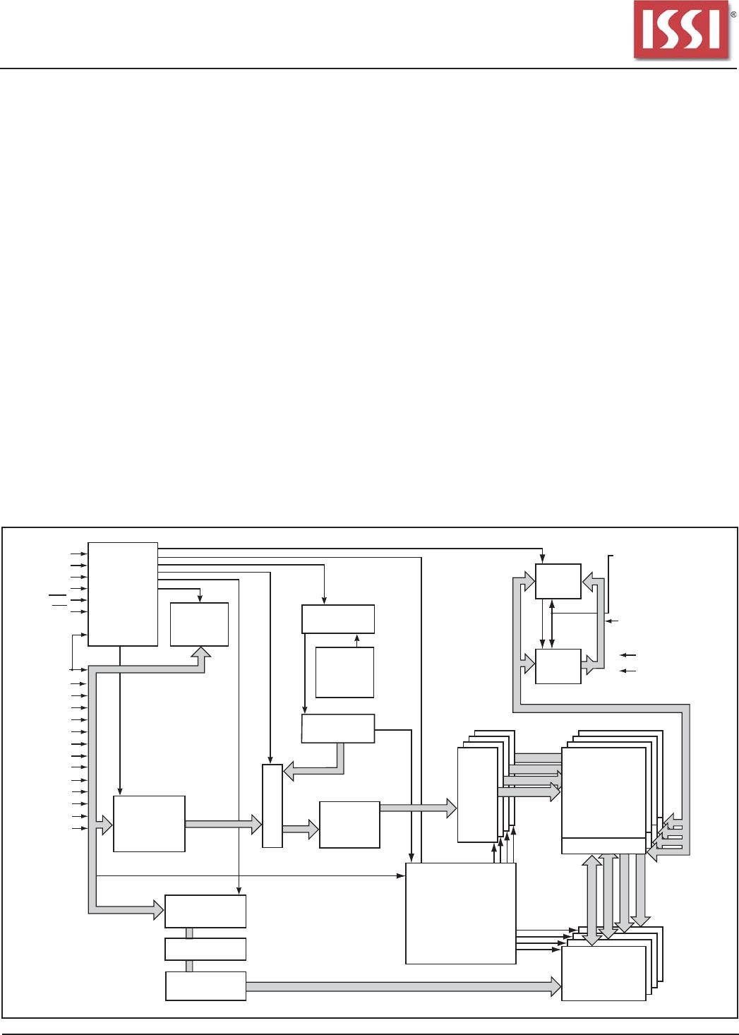
CLK
CKE
CS
RAS
CAS
WE
A9
A8
A7
A6
A5
A4
A3
A2
A1
A0
BA0
BA1
A10
COMMAND
DECODER
&
CLOCK
GENERATOR
MODE
REGISTER
REFRESH
CONTROLLER
REFRESH
COUNTER
SELF
REFRESH
CONTROLLER
ROW
ADDRESS
LATCH
MULTIPLEXER
COLUMN
ADDRESS LATCH
BURST COUNTER
COLUMN
ADDRESS BUFFER
COLUMN DECODER
DATA IN
BUFFER
DATA OUT
BUFFER
DQM0 - DQM3
DQ 0-31
V
DD
/V
DDQ
V
ss
/V
ssQ
12
12
8
12
12
8
32
32 32
32
256
(x 32)
4096
4096
4096
ROW DECODER
4096
MEMORY CELL
ARRAY
BANK 0
SENSE AMP I/O GATE
BANK CONTROL LOGIC
ROW
ADDRESS
BUFFER
A11
4
FUNCTIONAL BLOCK DIAGRAM (FOR 1MX32X4 BANKS)