PCA8546 All information provided in this document is subject to legal disclaimers. © NXP B.V. 2013. All rights reserved.
Product data sheet Rev. 1 — 13 November 2013 17 of 63
NXP Semiconductors
PCA8546
4 x 44 automotive LCD driver
8.2 Start-up and shut-down
8.2.1 Reset and Power-On Reset (POR)
After power-on the PCA8546 has to be initialized by sending the two bytes of the initialize
command (see Section 8.1.1
and Table 6).
After a reset and the initialization the starting conditions of the PCA8546 are as follows:
1. The display is disabled.
2. All backplane and segment outputs are set to V
SS
.
3. The data pointers are cleared (set logic 0).
4. RAM data is not initialized. Its content can be considered to be random.
5. The internal oscillator is running; no clock signal is available on pin OSCCLK; pin
OSCCLK is in 3-state.
The state after a reset and the initialization is shown in Table 20
.
After Power-On Reset (POR) and the initialize command and before enabling the display,
the RAM content should be brought to a defined state by writing meaningful content (for
example, a graphic) otherwise unwanted display artifacts may appear on the display.
8.2.2 RESET pin function
The RESET pin sets the PCA8546 in a defined mode. The RAM content remains
unchanged. After the reset signal is removed, the initialize command (see Section 8.1.1
and Table 6
) has to be sent to the PCA8546. See Section 8.2.1 for details.
8.2.3 Recommended start-up sequences
This chapter describes how to proceed with the initialization of the chip in different
application modes.
In general, the sequence should always be:
1. Power-on or reset the device,
2. send the initialize command,
3. set the display and functional modes,
4. fill the display memory and then
5. turn on the display.
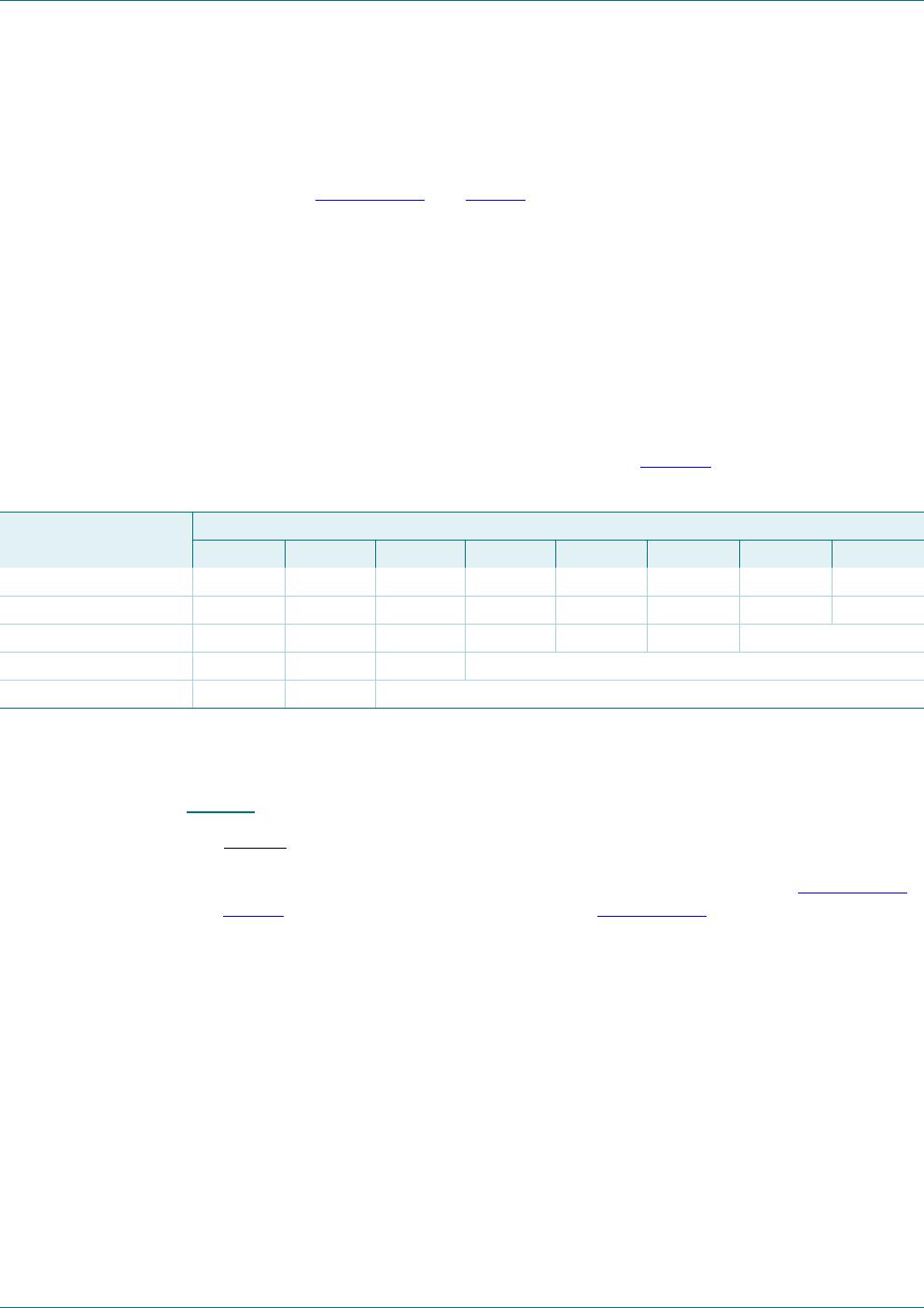
Table 20. Starting conditions
Associated command Bits
7 6 5 4 3 2 1 0
mode-settings - - - - BPS = 0 INV = 0 PD = 0 E = 0
oscillator-control - - - - - EFR = 0 COE = 0 OSC = 0
set-bias-mode - - - - - - B[1:0] = 00
frame-frequency - - - FD[4:0] = 01110
load-data-pointer - - DP[5:0] = 000000

