PCA8546 All information provided in this document is subject to legal disclaimers. © NXP B.V. 2013. All rights reserved.
Product data sheet Rev. 1 — 13 November 2013 34 of 63
NXP Semiconductors
PCA8546
4 x 44 automotive LCD driver
EMC detection: The PCA8546 is ruggedized against EMC susceptibility; however it is not
possible to cover all cases. To detect if a severe EMC event has occurred, it is possible to
check the responsiveness of the device by reading its register.
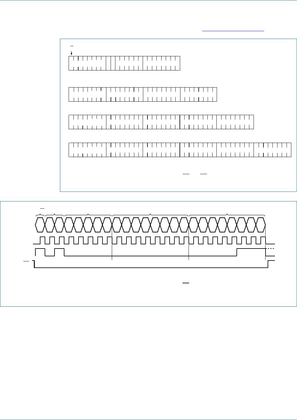
9.3 SPI-bus interface
Data transfer to the device is made via a 3 line SPI-bus (see Table 28). There is no output
data line. The SPI-bus is initialized whenever the chip enable line pin CE
is inactive.
[1] The chip enable must not be wired permanently LOW.
9.3.1 Data transmission
The chip enable signal is used to identify the transmitted data. Each data transfer is a byte
with the Most Significant Bit (MSB) sent first.
The transmission is controlled by the active LOW chip enable signal CE
. The first byte
transmitted is the subaddress byte.
The subaddress byte opens the communication with a read/write bit and a subaddress.
The subaddress is used to identify multiple devices on one SPI-bus.
Table 27. Modified status read out value
Bit Symbol Value Description
7 to 1 - 1111000 fixed value
0 A0 0 read back value is 1111 0000
1 read back value is 1111 0001
Table 28. Serial interface
Symbol Function Description
CE
chip enable input
[1]
; active LOW when HIGH, the interface is reset
SCL serial clock input input may be higher than V
DD
SDI serial data input input may be higher than V
DD
; input data is
sampled on the rising edge of SCL
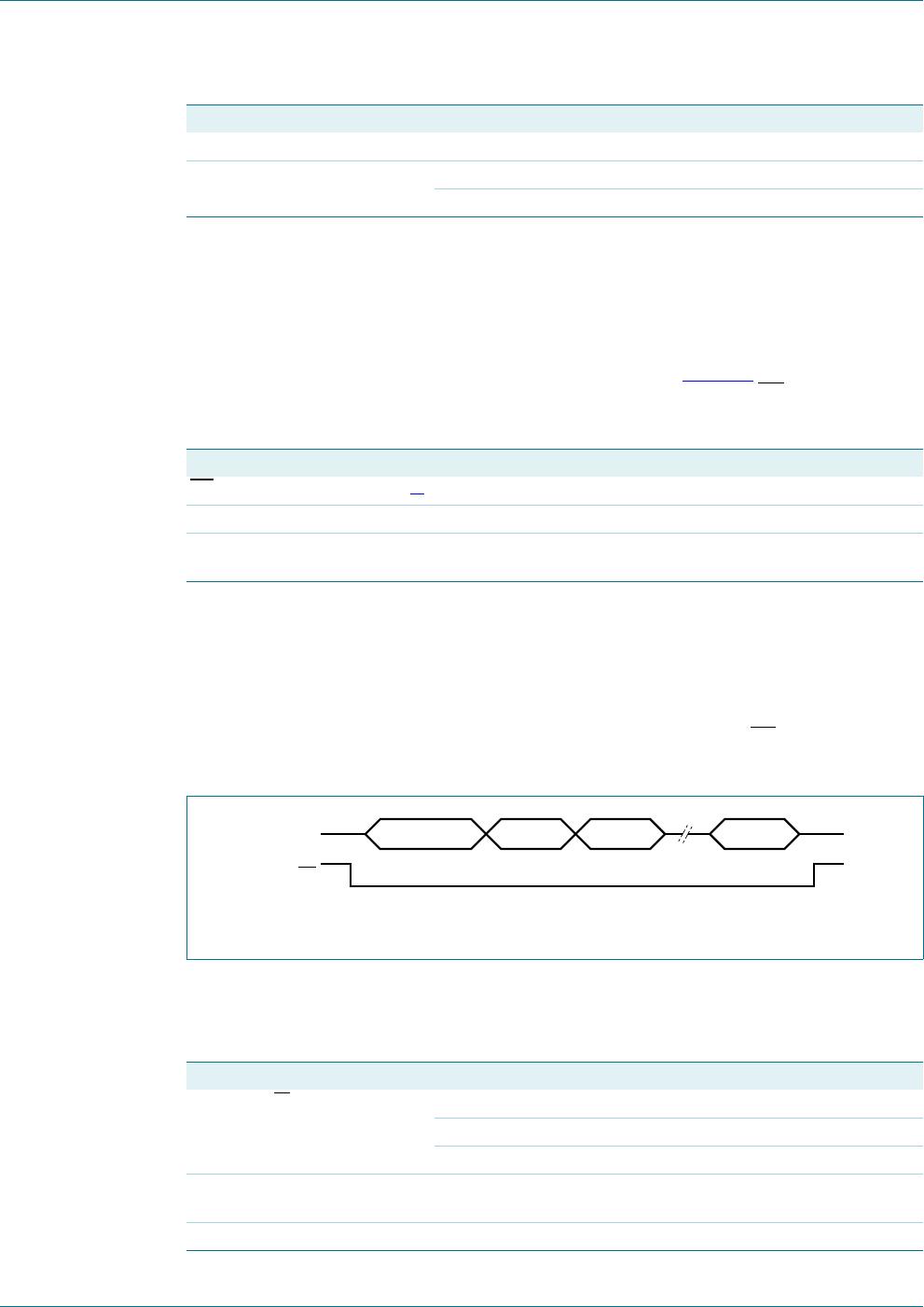
Fig 26. Data transfer overview
Table 29. Subaddress byte definition
Bit Symbol Value Description
7R/W
data read or write selection
0 write data
1 read data
6 to 5 SA[1:0] 01 subaddress; other codes cause the device to
ignore data transfer
4 to 0 - unused
&(
68%$''5(66 '$7$
'$7$ '$7$