13
COMMERCIAL AND INDUSTRIAL
TEMPERATURE RANGES
IDT72V3640/50/60/70/80/90 3.3V HIGH DENSITY SUPERSYNC II
TM
36-BIT FIFO
1,024 x 36, 2,048 x 36, 4,096 x 36, 8,192 x 36, 16,384 x 36 and 32,768 x 36
PROGRAMMING FLAG OFFSETS
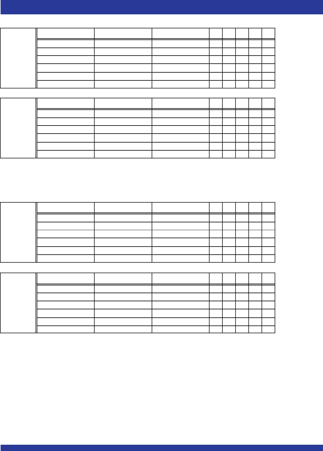
Full and Empty Flag offset values are user programmable. The IDT72V3640/
72V3650/72V3660/72V3670/72V3680/72V3690 have internal registers for
these offsets. There are eight default offset values selectable during Master
Reset. These offset values are shown in Table 2. Offset values can also be
programmed into the FIFO in one of two ways; serial or parallel loading method.
The selection of the loading method is done using the LD (Load) pin. During
Master Reset, the state of the LD input determines whether serial or parallel flag
offset programming is enabled. A HIGH on LD during Master Reset selects serial
loading of offset values. A LOW on LD during Master Reset selects parallel
loading of offset values.
In addition to loading offset values into the FIFO, it is also possible to read
the current offset values. Offset values can be read via the parallel output port
Q0-Qn, regardless of the programming mode selected (serial or parallel). It is
not possible to read the offset values in serial fashion.
Figure 3, Programmable Flag Offset Programming Sequence, summaries
the control pins and sequence for both serial and parallel programming modes.
For a more detailed description, see discussion that follows.
The offset registers may be programmed (and reprogrammed) any time after
Master Reset, regardless of whether serial or parallel programming has been
selected. Valid programming ranges are from 0 to D-1.
SYNCHRONOUS vs ASYNCHRONOUS PROGRAMMABLE FLAG
TIMING SELECTION
The IDT72V3640/72V3650/72V3660/72V3670/72V3680/72V3690 can
be configured during the Master Reset cycle with either synchronous or
asynchronous timing for PAF and PAE flags by use of the PFM pin.
If synchronous PAF/PAE configuration is selected (PFM, HIGH during
MRS), the PAF is asserted and updated on the rising edge of WCLK only and
not RCLK. Similarly, PAE is asserted and updated on the rising edge of RCLK
only and not WCLK. For detail timing diagrams, see Figure 17 for synchronous
PAF timing and Figure 18 for synchronous PAE timing.
If asynchronous PAF/PAE configuration is selected (PFM, LOW during
MRS), the PAF is asserted LOW on the LOW-to-HIGH transition of WCLK and
PAF is reset to HIGH on the LOW-to-HIGH transition of RCLK. Similarly, PAE
is asserted LOW on the LOW-to-HIGH transition of RCLK. PAE is reset to HIGH
on the LOW-to-HIGH transition of WCLK. For detail timing diagrams, see Figure
19 for asynchronous PAF timing and Figure 20 for asynchronous PAE timing.
IDT72V3640, 72V3650
LD FSEL1 FSEL0 Offsets n,m
LH L511
L L H 255
L L L 127
LH H63
HL L31
HH L15
HL H7
HH H3
LD FSEL1 FSEL0 Program Mode
H X X Serial
(3)
L X X Parallel
(4)
IDT72V3660, 72V3670, 72V3680, 72V3690
LD FSEL1 FSEL0 Offsets n,m
H L L 1,023
LH L511
L L H 255
L L L 127
LH H63
HH L31
HL H15
HH H7
LD FSEL1 FSEL0 Program Mode
H X X Serial
(3)
L X X Parallel
(4)
TABLE 2 — DEFAULT PROGRAMMABLE
FLAG OFFSETS
NOTES:
1. n = empty offset for PAE.
2. m = full offset for PAF.
3. As well as selecting serial programming mode, one of the default values will also
be loaded depending on the state of FSEL0 & FSEL1.
4. As well as selecting parallel programming mode, one of the default values will
also be loaded depending on the state of FSEL0 & FSEL1.