41
COMMERCIAL AND INDUSTRIAL
TEMPERATURE RANGES
IDT72V3640/50/60/70/80/90 3.3V HIGH DENSITY SUPERSYNC II
TM
36-BIT FIFO
1,024 x 36, 2,048 x 36, 4,096 x 36, 8,192 x 36, 16,384 x 36 and 32,768 x 36
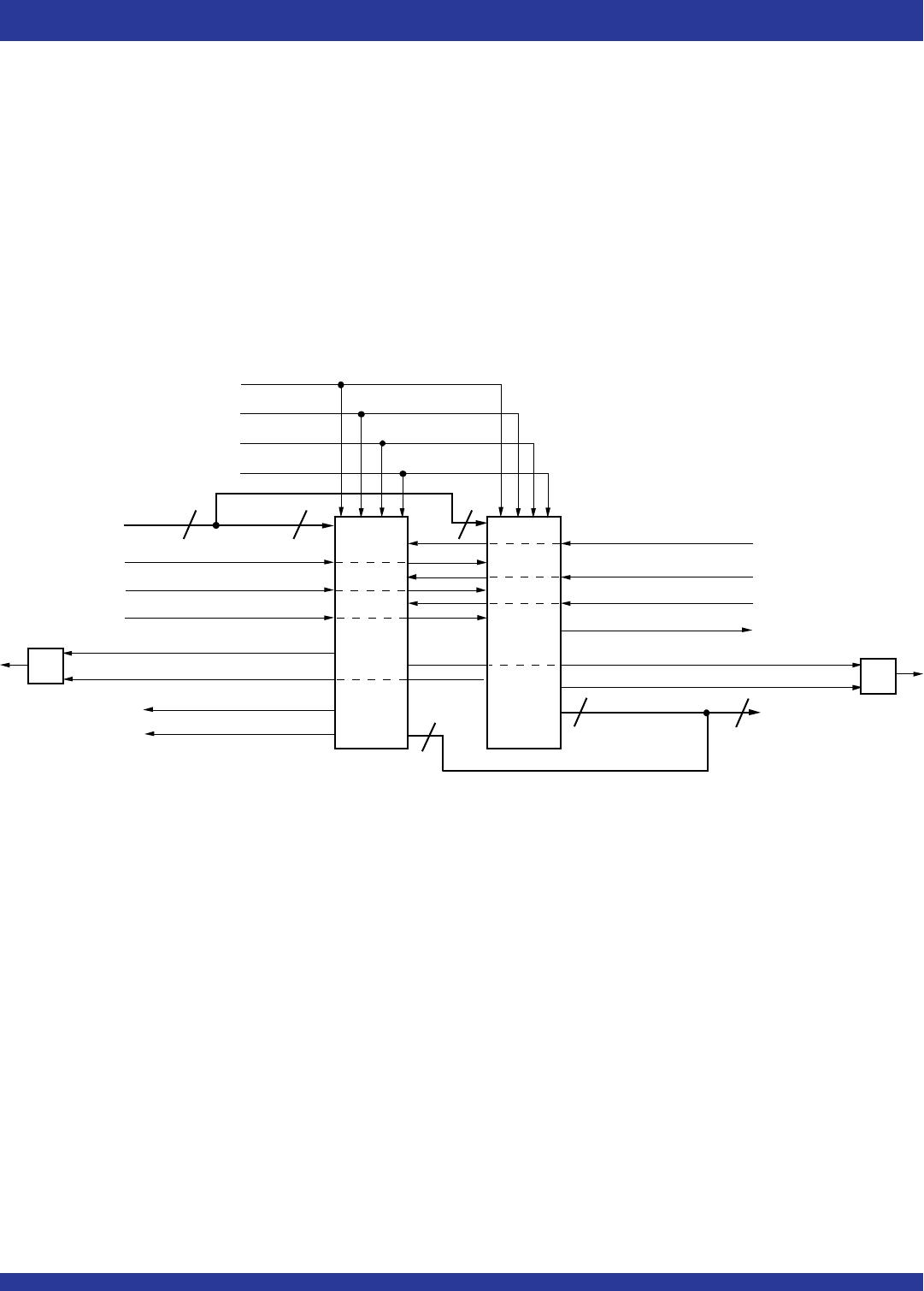
Figure 30. Block Diagram of 2,048 x 36, 4,096 x 36, 8,192 x 36, 16,384 x 36, 32,768 x 36 and 65,536 x 36 Depth Expansion
DEPTH EXPANSION CONFIGURATION (FWFT MODE ONLY)
The IDT72V3640 can easily be adapted to applications requiring depths
greater than 1,024, 2,048 for the IDT72V3650, 4,096 for the IDT72V3660,
8,192 for the IDT72V3670, 16,384 for the IDT72V3680 and 32,768 for the
IDT72V3690 with an 36-bit bus width. In FWFT mode, the FIFOs can be
connected in series (the data outputs of one FIFO connected to the data inputs
of the next) with no external logic necessary. The resulting configuration
provides a total depth equivalent to the sum of the depths associated with each
single FIFO. Figure 30 shows a depth expansion using two IDT72V3640/
72V3650/72V3660/72V3670/72V3680/72V3690 devices.
Care should be taken to select FWFT mode during Master Reset for all FIFOs
in the depth expansion configuration. The first word written to an empty
configuration will pass from one FIFO to the next ("ripple down") until it finally
appears at the outputs of the last FIFO in the chain – no read operation is
necessary but the RCLK of each FIFO must be free-running. Each time the data
word appears at the outputs of one FIFO, that device's OR line goes LOW,
enabling a write to the next FIFO in line.
For an empty expansion configuration, the amount of time it takes for OR of
the last FIFO in the chain to go LOW (i.e. valid data to appear on the last FIFO's
outputs) after a word has been written to the first FIFO is the sum of the delays
for each individual FIFO:
(N – 1)*(4*transfer clock) + 3*TRCLK
where N is the number of FIFOs in the expansion and TRCLK is the RCLK period.
Note that extra cycles should be added for the possibility that the tSKEW1
specification is not met between WCLK and transfer clock, or RCLK and transfer
clock, for the OR flag.
The "ripple down" delay is only noticeable for the first word written to an empty
depth expansion configuration. There will be no delay evident for subsequent
words written to the configuration.
The first free location created by reading from a full depth expansion
configuration will "bubble up" from the last FIFO to the previous one until it finally
moves into the first FIFO of the chain. Each time a free location is created in one
FIFO of the chain, that FIFO's IR line goes LOW, enabling the preceding FIFO
to write a word to fill it.
For a full expansion configuration, the amount of time it takes for IR of the first
FIFO in the chain to go LOW after a word has been read from the last FIFO is
the sum of the delays for each individual FIFO:
(N – 1)*(3*transfer clock) + 2 T
WCLK
where N is the number of FIFOs in the expansion and TWCLK is the WCLK
period. Note that extra cycles should be added for the possibility that the tSKEW1
specification is not met between RCLK and transfer clock, or WCLK and transfer
clock, for the IR flag.
The Transfer Clock line should be tied to either WCLK or RCLK, whichever
is faster. Both these actions result in data moving, as quickly as possible, to the
end of the chain and free locations to the beginning of the chain.
Dn
INPUT READY
WRITE ENABLE
WRITE CLOCK
WEN
WCLK
IR
DATA IN
RCLK
READ CLOCK
RCLK
REN
OE
OUTPUT ENABLE
OUTPUT READY
Qn
Dn
IR
GND
WEN
WCLK
OR
REN
OE
Qn
READ ENABLE
OR
DATA OUT
IDT
72V3640
72V3650
72V3660
72V3670
72V3680
72V3690
TRANSFER CLOCK
4667 drw 35
n
n n
FWFT/SI FWFT/SI
FWFT/SI
IDT
72V3640
72V3650
72V3660
72V3670
72V3680
72V3690