10
INDUSTRIAL TEMPERATURE RANGE
IDT5V9885T
3.3V EEPROM PROGRAMMABLE CLOCK GENERATOR
Example
FIN = 25MHz, FOUT = 100MHz, Fssc = 33KHz with center spread of ±2%. Find the necessary spread spectrum register settings.
Since the spread is center, the SS_OFFSET can be set to '0'. Solve for the nominal M value; keep in mind that the nominal M should be chosen to maximize
the VCO. Start with D = 1, using Eq.10 and Eq.11.
MNOM = 1200MHz / 25MHz = 48
Using Eq.4, we arbitrarily choose N = 22, A = 3. Now that we have the nominal M value, we can determine TSSC and NSSC by using Eq.12.
Nssc * Tssc = 25MHz / (33KHz * 4) = 190
However, using Eq. 7 and Eq.8, we find that the closest value is when TSSC = 14 and NSSC = 6. Keep in mind to maximize the number of samples used
to enhance the profile of the spread spectrum waveform.
Tssc = 14 + 2 = 16
Nssc = 6 * 2 = 12
Nssc * Tssc = 192
Use Eq.14 to determine the value of the sigma-delta-encoded samples.
±2% = ΣΔ * 100
64 * 48
ΣΔ = 61.44
Either round up or down to the nearest integer value. Therefore, we end up with 61 or 62 for sigma-delta-encoded samples. Since the sigma-delta-encoded
samples must not exceed 63 with SS_OFFSET set to '0', 61 or 62 is well within the limits. It is the discretion of the user to define the shape of the profile that
is better suited for the intended application.
Using Eq.14 again, the actual spread for the sigma-delta-encoded samples of 61 and 62 are ±1.99% and ±2.02%, respectively.
Use Eq.10 to determine if the X2 bit needs to be set;
Amplitude = 48 * (1.99 or 2.02) / 100 = 0.48 < 1
2
Therefore, the X2 = '0 '. The dither bit is left to the discretion of the user.
The example above was of a center spread using spread spectrum. For down spread, the nominal M value can be set one integer value lower to 43.
Note that the 5V9885T should not be programmed with TSSC > '0', SS_OFFSET = '0', and SD = '0' in order to prevent an unstable state in the modulator.
The PLL loop bandwidth must be at least 10x the modulation frequency along with higher damping (larger ωuz) to prevent the spread spectrum from being filtered
and reduce extraneous noise. Refer to the LOOP FILTER section for more detail on ωuz. The A[3:0] must be used for spread spectrum, even if the total multiplier
value is an even integer.
FRACTIONAL DIVIDER
There is the option for the feedback-divider to be programmed as a fractional divider for only PLL0 and PLL. By setting TSSC > '0' and SD bits to '0', the
SS_OFFSET bits would determine the fractional divide value. See the SPREAD SPECTRUM GENERATION section for more details on the TSSC, SD, and
SS_OFFSET bits. The following equation governs how the fractional divide value is set.
M = 2*N[11:0] + A[3:0] + 1 + SS_OFFSET[5:0] *1/64
11
INDUSTRIAL TEMPERATURE RANGE
IDT5V9885T
3.3V EEPROM PROGRAMMABLE CLOCK GENERATOR
The spread spectrum parameters such as the modulation frequency and profile will not be enabled nor will it have any impact on the PLL output when the
PLL is programmed for fractional divide.
The following is an example of how to set the fractional divider.
Example
FIN = 20MHz, FOUT1 = 168.75MHz, FOUT2 = 350MHz
Solving for 350MHz using Eq.2 and Eq.3 with PLL0 and spread spectrum off,
350MHz = 20MHz * (M / D)/ (P * 2)
For better jitter performance, keep D as small as possible
(350MHz * 2/20MHz)= (M/P) = 35
Therefore, we have D = 1, M = 35 (N = 16, A = 2) for PLL0 with P = 1 on output bank4 resulting in 350MHz.
Solving for 168.75MHz with PLL1 and fractional divide enabled:
168.75MHz = 20MHz * (M / D)/(P * 2)
168.75MHz * 2/20MHz = M/P = 16.875/1 or 33.75/2
The 33.75 value is chosen to achieve the highest VCO frequency possible. Next step is to figure out the setting for the fractional divide using Eq.3.
33.75 = 2*N + A + 1 + SS_OFFSET * 1/64
Integer value 33 can be determined by N and A, thus leaving 0.75 left to be solved.
2*N + A + 1 = 33
SS_OFFSET = 64 * 0.75 = 48
Therefore, we have D=1, M=33.75 (N=15, A=2, SS_OFFSET=48) for PLL1 with P=2 on an output bank resulting in 168.75MHz.
The fractional divider can be determined if it is needed by following the steps in the previous example. Note that the 5V9885T should not be programmed
with TSSC > '0', SS_OFFSET = '0', and SD = '0' in order to prevent an unstable state in the modulator. The A[3:0] must be used and set to be greater than
'2' for a more accurate fractional divide.
12
INDUSTRIAL TEMPERATURE RANGE
IDT5V9885T
3.3V EEPROM PROGRAMMABLE CLOCK GENERATOR
LOOP FILTER
The loop filter for each PLL can be programmed to optimize the jitter performance. The low-pass frequency response of the PLL is the mechanism that dictates
the jitter transfer characteristics. The loop bandwidth can be extracted from the jitter transfer. A narrow loop bandwidth is good for jitter attenuation while a wide
loop bandwidth is best for low jitter generation. The specific loop filter components that can be programmed are the resistor via the RZ[3:0] bits, pole capacitor
via the CZ[3:0] bits, zero capacitor via the CP[3:0] bits, and the charge pump current via the IP[2:0] bits.
The following equations govern how the loop filter is set.
Resistor (Rz) = 0.3KΩ + RZ[3:0] * 1KΩ (Eq. 15)
Zero capacitor (Cz) = 6pF + CZ[3:0] * 27.2pF (Eq. 16)
Pole capacitor (Cp) = 1.3pF + CP[3:0] * 0.75pF (Eq. 17)
Charge pump current (Ip) = 5 * 2
IP[2:0]
μA (Eq. 18)
Parameter Bits Step Min Max Units
RZ 4 1 0.3 15.3 K Ω
CZ 4 27.2 6 414 pF
CP 4 0.75 1.3 12.55 pF
IP 3 2
n
5 640 μA
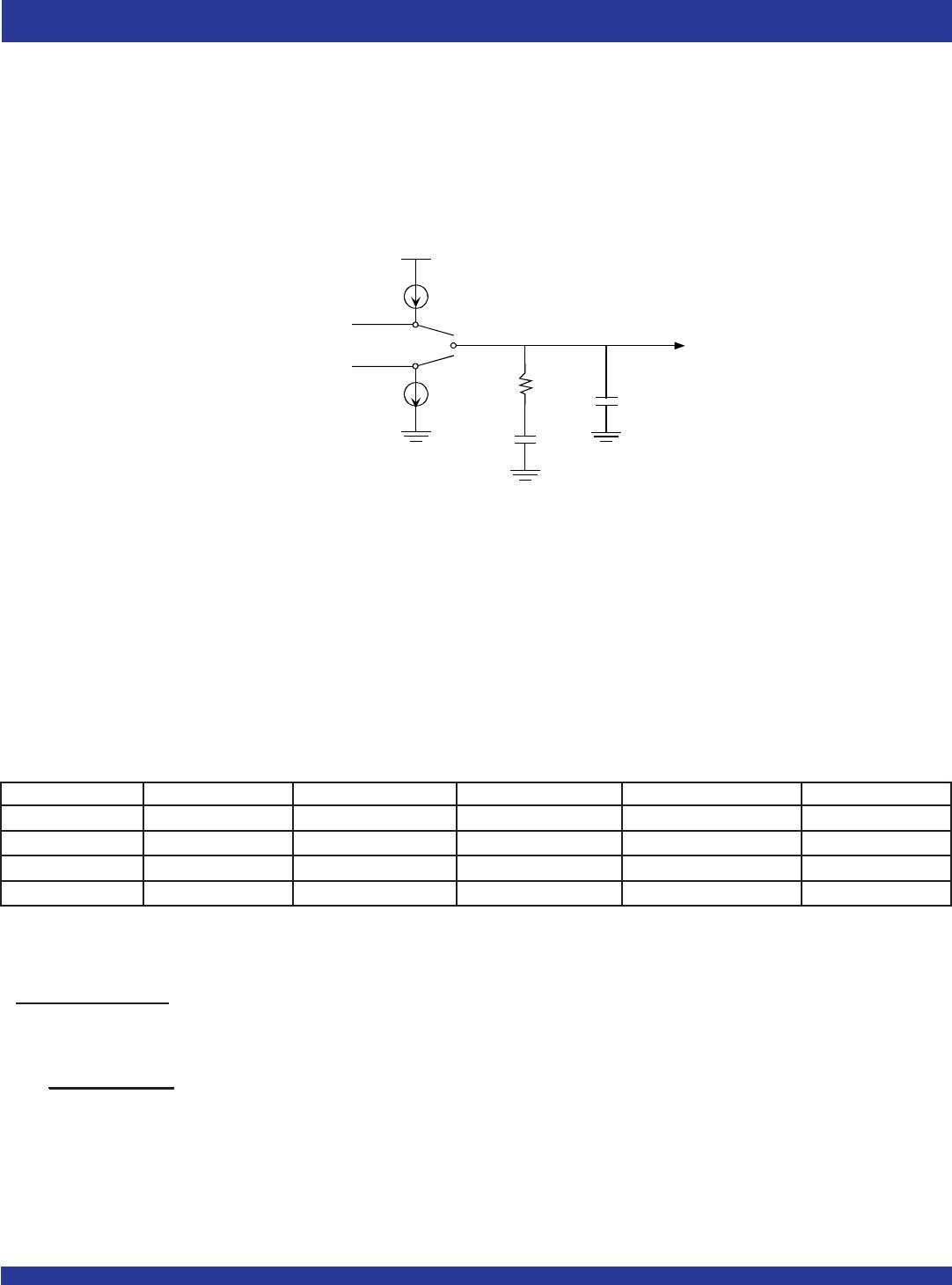
From PFD
V
DD
UP
Ip
DOWN
Ip
Rz
Cz
Cp
To VCO
Charge Pump and Loop Filter Configuration
PLL loop filter design is beyond the scope of this datasheet. Refer to design procedures for 3-order charge-pump based PLLs. For the sake of simplicity,
the fastest and easiest way to calculate the PLL loop bandwidth (Fc) given the programmable loop filter parameters is as follows.
PLL Loop Bandwidth:
Charge pump gain (Kφ) = Ip / 2π (Eq. 19)
VCO gain (KVCO) = 950MHz/V * 2π (Eq. 20)
M = Total multiplier value (See the PRE-SCALERS, FEEDBACK-DIVIDERS, POST-DIVIDERS section for more detail)
ωc = Rz * Kφ * KVCO * Cz (Eq. 21)
M * (Cz + Cp)
Fc = ωc / 2π (Eq. 22)
Note, the phase/frequency detector frequency (FPFD) is typically seven times the PLL closed-loop bandwidth (Fc) but too high of a ratio will reduce your
phase margin thus compromising loop stability.

5V9885TPFGI8

Mfr. #:
Manufacturer:
IDT
Description:
Clock Generators & Support Products SPREAD SPECTRUM PROG . CLK
Lifecycle:
New from this manufacturer.
Delivery:
DHL FedEx Ups TNT EMS
Payment:
T/T Paypal Visa MoneyGram Western Union

Products related to this Datasheet