25
INDUSTRIAL TEMPERATURE RANGE
IDT5V9885T
3.3V EEPROM PROGRAMMABLE CLOCK GENERATOR
Standard JTAG Timing
NOTE:
t1 = tTCLKLOW
t2 = tTCLKHIGH
t3 = tTCLKFALL
t4 = tTCLKRISE
t5 = tRST (reset pulse width)
t6 = tRSR (reset recovery)
TCLK
TDI/TMS
TDO
TRST
t
TCLK
t1
t2
t3
t4
t5
t6
t
DS tDH
tDO
TDO
JTAG
AC ELECTRICAL CHARACTERISTICS
NOTE:
1. Guaranteed by design.
SYSTEM INTERFACE PARAMETERS
Symbol Parameter Min. Max. Units
tDO Data Output
(1)
—20ns
tDOH Data Output Hold
(1)
0 ns
tDS Data Input, tRISE = 3ns 10 ns
tDH Data Input, tFALL = 3ns 10 ns
NOTE:
1. 50pF loading on external output signals.
Symbol Parameter Min. Max. Units
tTCLK JTAG Clock Input Period 100 ns
tTCLKHIGH JTAG Clock HIGH 40 ns
tTCLKLOW JTAG Clock Low 40 ns
tTCLKRISE JTAG Clock Rise Time 5
(1)
ns
tTCLKFALL JTAG Clock Fall Time 5
(1)
ns
tRST JTAG Reset 50 ns
tRSR JTAG Reset Recovery 50 ns
In order for the save and restore instructions to function properly, the IDT5V9885T must not be in shutdown mode (SHUTDOWN pin asserted). In the event
of an interrupt of some sort such as a power down of the part in the middle of a save or restore operation, the contents to or from the EEPROM will be partially
loaded, and a CRC error will be generated. The CERR bit (0x81) will be asserted to indicate that an error has occurred. The LOSS_LOCK signal will also
be asserted.
On power-up of the IDT5V9885T, an automatic restore is performed to load the EEPROM contents into the internal programming registers. The auto-restore
will not function properly if the device is in shutdown mode (SHUTDOWN pin asserted). The IDT5V9885T will be ready to accept a programming instruction
once it acknowledges its 7-bit I
2
C address.
26
INDUSTRIAL TEMPERATURE RANGE
IDT5V9885T
3.3V EEPROM PROGRAMMABLE CLOCK GENERATOR
I
2
C BUS DC CHARACTERISTICS
Symbol Parameter Conditions Min Typ Max Unit
VIH Input HIGH Level 0.7 * VDD V
VIL Input LOW Level 0.3 * VDD V
VHYS Hysteresis of Inputs 0.05 * VDD V
IIN Input Leakage Current ±1.0 μA
VOL Output LOW Voltage IOL = 3 mA 0.4 V
I
2
C BUS AC CHARACTERISTICS FOR STANDARD MODE
Symbol Parameter Min Typ Max Unit
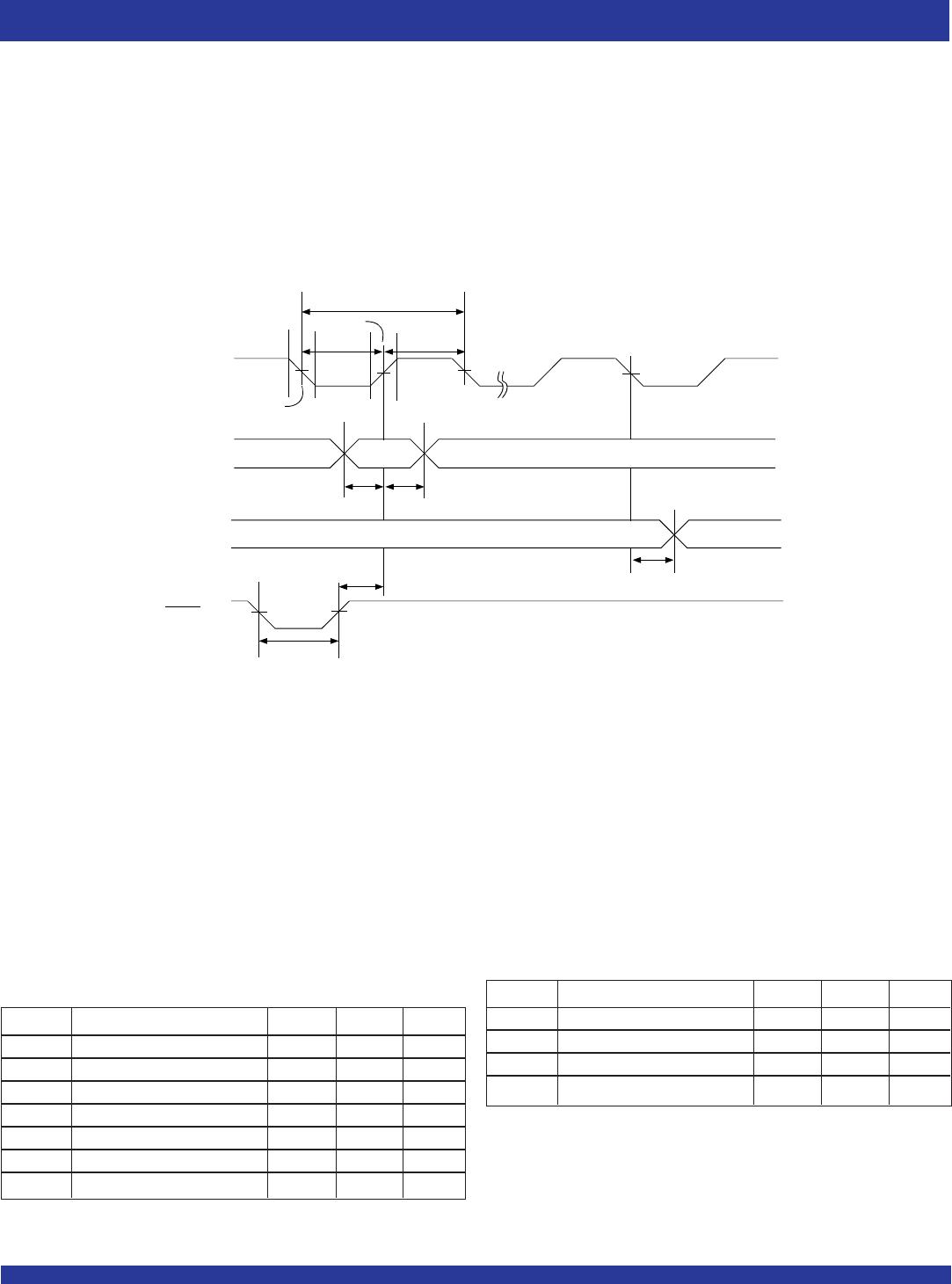
FSCLK Serial Clock Frequency (SCLK) 0 100 KHz
tBUF Bus free time between STOP and START 4.7 μs
tSU:START Setup Time, START 4.7 μs
tHD:START Hold Time, START 4 μs
tSU:DATA Setup Time, data input (SDAT) 250 ns
tHD:DATA Hold Time, data input (SDAT)
(1)
0 μs
tOVD Output data valid from clock 3.45 μs
CB Capacitive Load for Each Bus Line 400 pF
tR Rise Time, data and clock (SDAT, SCLK) 1000 ns
tF Fall Time, data and clock (SDAT, SCLK) 300 ns
tHIGH HIGH Time, clock (SCLK) 4 μs
tLOW LOW Time, clock (SCLK) 4.7 μs
t
SU:STOP Setup Time, STOP 4 μs
I
2
C BUS AC CHARACTERISTICS FOR FAST MODE
Symbol Parameter Min Typ Max Unit
FSCLK Serial Clock Frequency (SCLK) 0 400 KHz
tBUF Bus free time between STOP and START 1.3 μs
tSU:START Setup Time, START 0.6 μs
tHD:START Hold Time, START 0.6 μs
tSU:DATA Setup Time, data input (SDAT) 100 ns
tHD:DATA Hold Time, data input (SDAT)
(1)
0 μs
tOVD Output data valid from clock 0.9 μs
CB Capacitive Load for Each Bus Line 400 pF
tR Rise Time, data and clock (SDAT, SCLK) 20 + 0.1 * CB 300 ns
tF Fall Time, data and clock (SDAT, SCLK) 20 + 0.1 * CB 300 ns
tHIGH HIGH Time, clock (SCLK) 0.6 μs
tLOW LOW Time, clock (SCLK) 1.3 μs
t
SU:STOP Setup Time, STOP 0.6 μs
NOTE:
1. A device must internally provide a hold time of at least 300ns for the SDAT signal (referred to the VIHMIN of the SCLK signal) to bridge the undefined region of the falling edge
of SCLK.
NOTE:
1. A device must internally provide a hold time of at least 300ns for the SDAT signal (referred to the VIHMIN of the SCLK signal) to bridge the undefined region of the falling edge
of SCLK.
27
INDUSTRIAL TEMPERATURE RANGE
IDT5V9885T
3.3V EEPROM PROGRAMMABLE CLOCK GENERATOR
Symbol Description Max Unit
VDD Internal Power Supply Voltage -0.5 to +4.6 V
VI Input Voltage -0.5 to +4.6 V
VO Output Voltage
(2)
-0.5 to VDD + 0.5 V
TJ Junction Temperature 150 °C
T
STG Storage Temperature –65 to +150 °C
ABSOLUTE MAXIMUM RATINGS
(1)
NOTE:
1. Stresses greater than those listed under ABSOLUTE MAXIMUM RATINGS may cause
permanent damage to the device. This is a stress rating only and functional operation
of the device at these or any other conditions above those indicated in the operational
sections of this specification is not implied. Exposure to absolute maximum rating
conditions for extended periods may affect reliability.
2. Not to exceed 4.6V.
NOTE:
1. Capacitance levels characterized but not tested.
Symbol Parameter Min. Typ. Max. Unit
C
IN Input Capacitance 4 pF
Crystal Specifications
XTAL_FREQ Crystal Frequency 8 50 MHz
XTAL_MIN Minimum Crystal Load Capacitance 3.5 pF
XTAL_MAX Maximum Crystal Load Capacitance 35.4 pF
Crystal Load Capacitance Resolution 0.125
XTAL_V
PP Voltage Swing (peak-to-peak, nominal) 2.3 V
CAPACITANCE (TA = +25°C, f = 1MHz, VIN = 0V)
(1)
Symbol Description Min. Typ. Max. Unit
V
DD Power Supply Voltage for LVTTL 3 3.3 3.6 V
Power Supply Voltage for LVDS/LVPECL 3.135 3.3 3.465
TA Operating Temperature, Ambient 40 +85 ° C
CLOAD_OUT Maximum Load Capacitance (LVTTL only) 15 pF
F
IN External Reference Crystal 8 50 MHz
External Reference Clock, Industrial 1 400
t
PU Power-up time for all VDDs to reach minimum specified voltage 0.05 5 ms
(power ramps must be monotonic)
RECOMMENDED OPERATING CONDITIONS

5V9885TPFGI8

Mfr. #:
Manufacturer:
IDT
Description:
Clock Generators & Support Products SPREAD SPECTRUM PROG . CLK
Lifecycle:
New from this manufacturer.
Delivery:
DHL FedEx Ups TNT EMS
Payment:
T/T Paypal Visa MoneyGram Western Union

Products related to this Datasheet