20
INDUSTRIAL TEMPERATURE RANGE
IDT5V9885T
3.3V EEPROM PROGRAMMABLE CLOCK GENERATOR
POWER UP AND POWER SAVING FEATURES
If a global shutdown is enabled, SHUTDOWN pin asserted, most of the chip except for the PLLs will be powered down. In order to have a complete
power down of the chip, the PLLs must be powered down via the SUSPEND function or by setting the pre-scaler bits to '0x00' and disable the internal
GINx signals via the enable bits at memory address 0x05. Note that the register bits will not lose their state in the event of a chip power-down. The only
possibility that the register bits will lose their state is if the part was power-cycled. After coming out of shutdown mode, the PLLs will require time to relock.
During power up, the values of GIN4, GIN3, GIN2, GIN1 and GIN0 will be latched and used for PLL configuration selection, regardless of the state of the
I
2
C/JTAG pin and GINx being disabled via the GINENx bits. GIN5 will have an internal state of LOW. The GIN pins should be held LOW during power up
to select configuration0 as default. The output levels will be at an undefined state during power up.
The post-divider should never be disabled via PM bits after power up, or else it will render the output bank completely non-functional during normal
operation, (unless the output bank itself will not be used at all).
During power up, the VDD ramp must be monotonic.
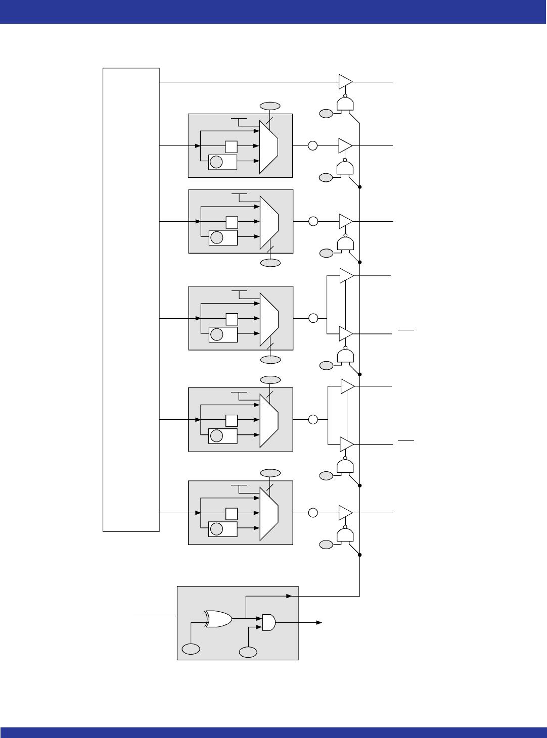
LOSS OF LOCK AND INPUT CLOCK
The device employs a loss of lock and loss of input clock detection circuitry. The GOUT0/LOSS_LOCK and GOUT1/LOSS_CLKIN are the outputs that
indicate such failures. LOSS_LOCK signal will be asserted if any of the three powered up PLLs loses frequency lock for any event other than PLL
shutdown. Lock is determined by checking that the reference and feedback clocks are within 1/2 period of each other.Loss_LOCK signal may be falsely
asserted when
- Spread Spectrum is turned on for any of the PLLs
- Fractional divider is used for any of the PLLs
- the reference and feedback clocks are not within 1/2 period of each other.
LOSS_CLKIN is asserted when the currently selected clock is lost or is asserted when both clocks are lost. In the event of the selected clock being
absent up on power up, the loss of the selected clock detection circuitry will reference an internal oscillator. LOSS_LOCK and LOSS_CLKIN cannot be
used as reliable inputs to other devices.
SWITCHOVER MODES
The IDT5V9885T features redundant clock inputs which supports both Automatic and Manual switchover mode. These two modes are determined by
the configuration bits, SM (0x34). The primary clock source can be programmed, via the PRIMCLK bit, to be either XTALIN/REFIN or CLKIN, which is
determined by the PRIMCLK bit. The other clock source input will be considered as the secondary source. This is more detailed in the 'REFERENCE
CLOCK INPUT PINS AND SELECTION'. Note that the switchover modes are asynchronous. If the reference clocks are directly routed to OUTx with no
phase relationship, short pulses can be generated during switchover. The automatic switchover mode will work only when the primary clock source is
XTALIN/REFIN.
MANUAL SWITCHOVER MODE
When SM[1:0] is "0x", the redundant inputs are in manual switchover mode. In this mode, CLK_SEL pin is used to switch between the primary and
secondary clock sources. As previously mentioned, the primary and secondary clock source setting is determined by the PRIMCLK bit. During the
switchover, no glitches will occur at the output of the device, although there may be frequency and phase drift, depending on the exact phase and
frequency relationship between the primary and secondary clocks. If GOUT1 is used as LOSS_CLKIN, it indicates loss of primary clock.
AUTOMATIC SWITCHOVER MODE
When SM[1:0] is "11", the redundant inputs are in automatic revertive switchover mode.