24
INDUSTRIAL TEMPERATURE RANGE
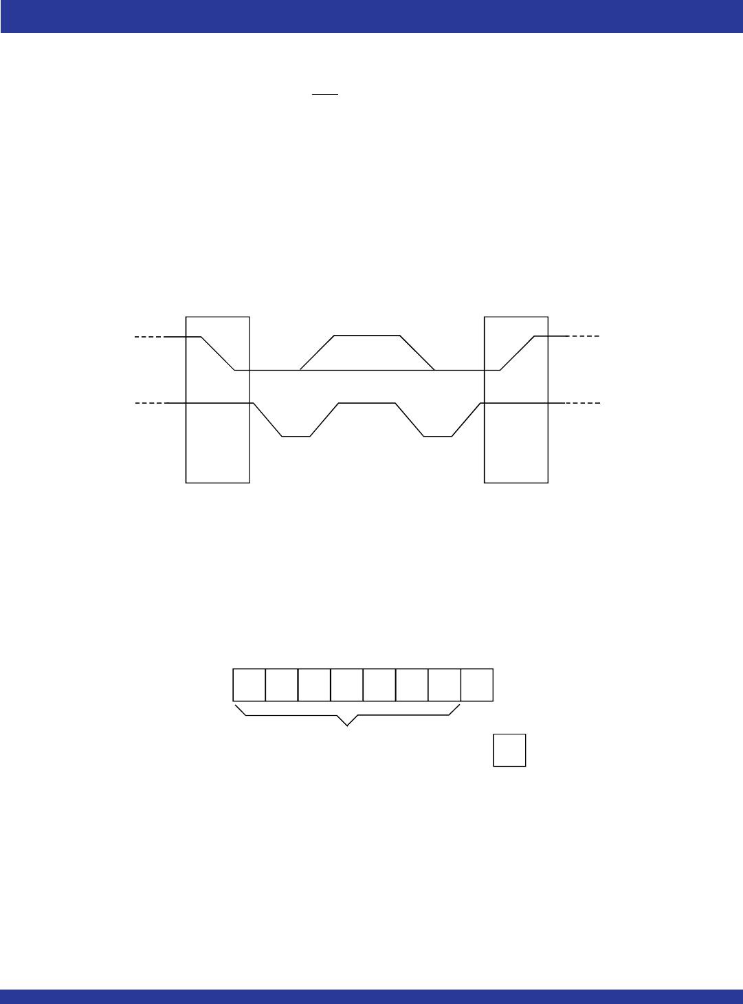
IDT5V9885T
3.3V EEPROM PROGRAMMABLE CLOCK GENERATOR
EEPROM INTERFACE
The IDT5V9885T can also store its configuration in an internal EEPROM. The contents of the device's internal programming registers can be saved to the
EEPROM by issuing a save instruction (ProgSave) and can be loaded back to the internal programming registers by issuing a restore instruction (ProgRestore).
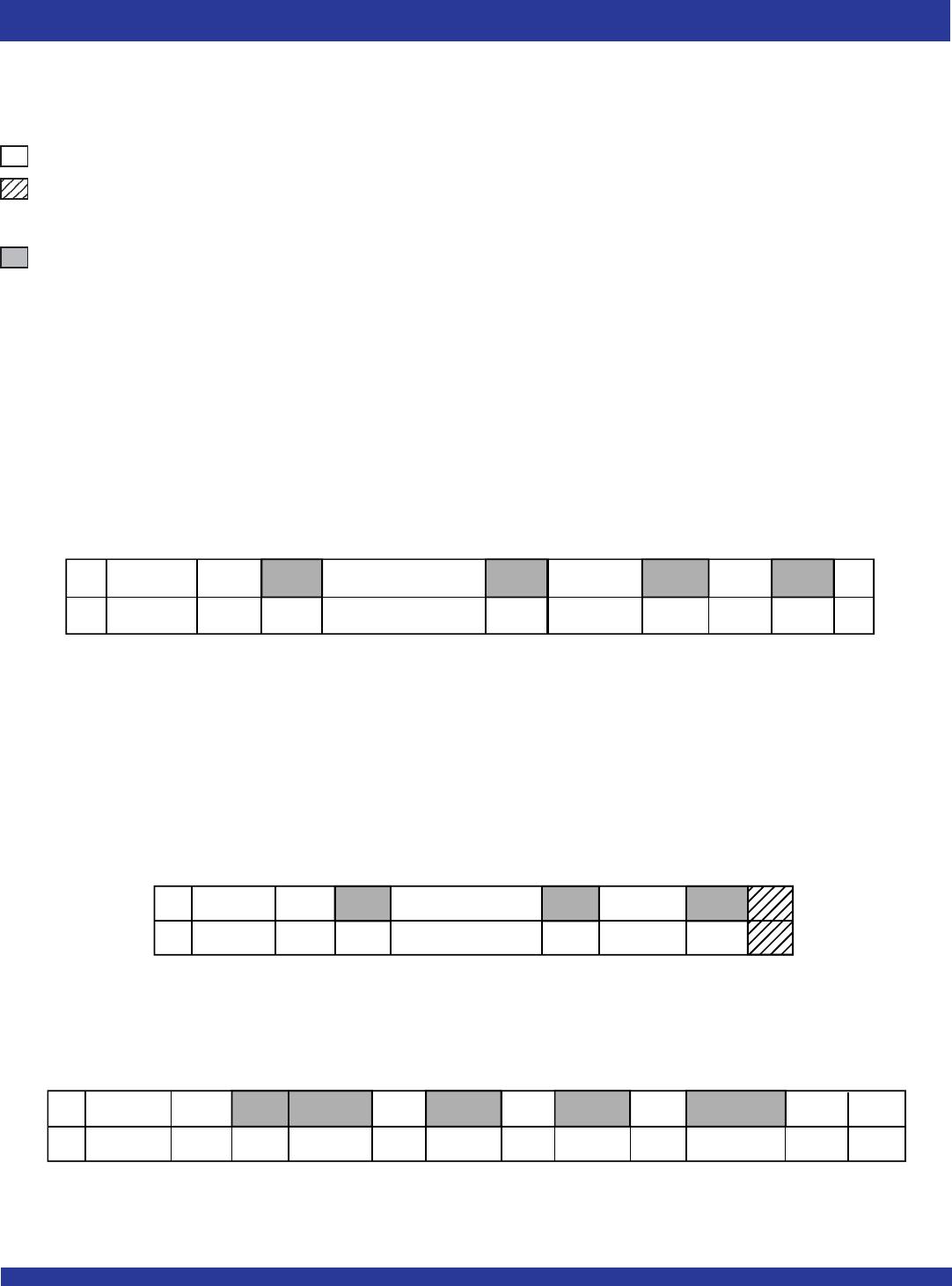
To initiate a save or restore using I
2
C, only two bytes are transferred. The Device Address is issued with the read/write bit set to "0", followed by the appropriate
command code. The save or restore instruction executes after the STOP condition is issued by the Master, during which time the IDT5V9885T will not generate
Acknowledge bits. The IDT5V9885T will acknowledge the instructions after it has completed execution of them. During that time, the I
2
C bus should be interpreted
as busy by all other users of the bus.
Using JTAG, the ProgSave and ProgRestore instructions selects the BYPASS register path for shifting the data from TDI to TDO during the data register scanning.
During the execution of a ProgSave or ProgRestore instruction, the IDT5V9885T will not accept a new programming instruction (read, write, save, or restore).
All non-programming JTAG instructions will function properly, but the user should wait until the save or restore is complete before issuing a new programming
instruction. If a new programming instruction is issued before the save or restore completes, the new instruction is ignored, and the BYPASS register path remains
in effect for shifting data from TDI to TDO during data register scanning.
The time it takes for the save (TSAVE) and restore (TRESTORE) instructions to complete is:
TSAVE = 100ms max, TRESTORE = 10 ms max
PROGSAVE
PROGRESTORE
NOTE:
PROGWRITE is for writing to the 5V9885T registers.
PROGREAD is for reading the 5V9885T registers.
PROGSAVE is for saving all the contents of the 5V9885T registers to the EEPROM.
PROGRESTORE is for loading the entire EEPROM contents to the 5V9885T registers.
S Address R/W ACK Command Code ACK
7-bits 0 1-bit 8-bits:xxxxxx01
1-bit
P
S Address R/W ACK Command Code ACK
7-bits 0 1-bit 8-bits:xxxxxx10
1-bit
P
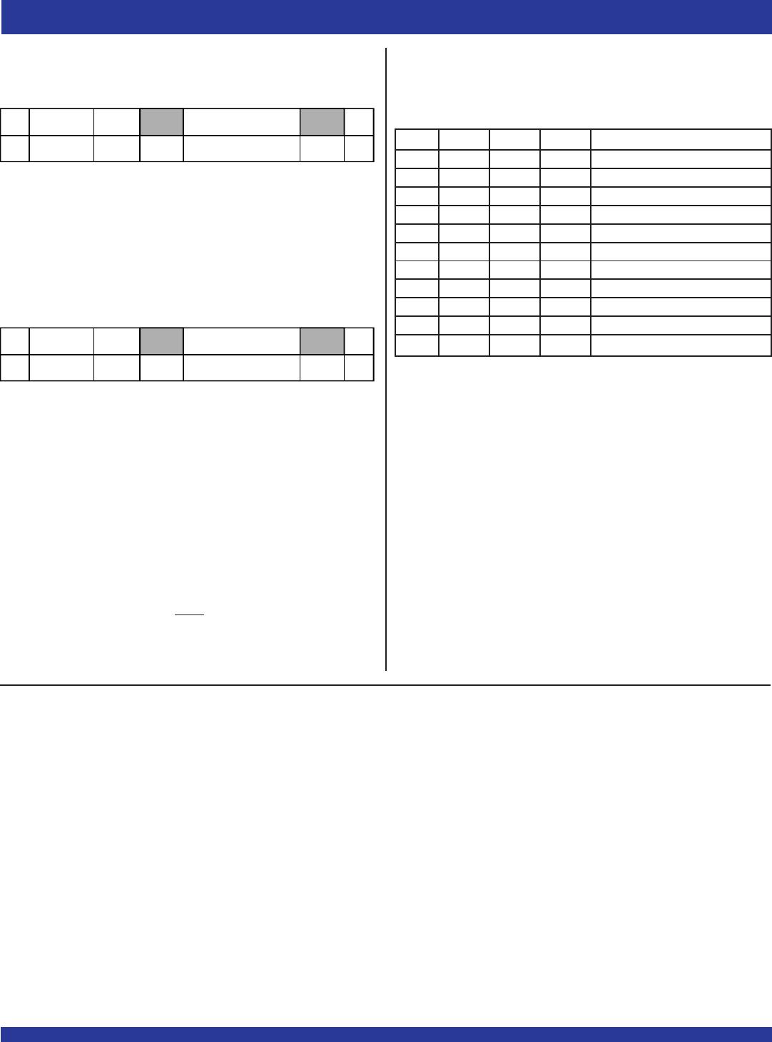
JTAG INTERFACE
In addition to the IEEE 1149.1 instructions EXTEST, SAMPLE/PRELOAD,
CLAMP, HIGH-Z and BYPASS, the 5V9885T allows access to internal
programming registers using the REGADDR (set register address), REGDATAR
(read register) and REGDATW (write register instructions. Data is always
accessed by byte, and the register address increments after each read or write.
The full instruction set follows. The IDT5V9885T will be updating the registers
during programming.
The JTAG TAP controller can be reset in one of four ways:
1) Power up in JTAG mode
2) Power up in I
2
C mode and then go into JTAG mode, or go out of and back
into JTAG mode with the I
2
C/JTAG pin
3) Apply TRST while in JTAG mode
4) Apply five rising edges of TCK with TMS high while in JTAG mode
IR (3) IR (2) IR (1) IR (0) Instructions
0 0 0 0 EXTEST
(1)
0 0 0 1 SAMPLE/PRELOAD
(1)
0 0 1 0 IDCODE
(1)
0 0 1 1 REGADDR
(2)
0 1 0 0 REGDATAW / PROGWRITE
(3)
0 1 0 1 REGDATAR / PROGREAD
(4)
0 1 1 0 PROGSAVE
(5)
0 1 1 1 PROGRESTORE
(6)
1 0 0 0 CLAMP
(1)
1 0 0 1 HIGHZ
(1,7)
1 1 1 1 BYPASS
(1)
JTAG INSTRUCTION REGISTER
DESCRIPTION
NOTES:
1. IEEE 1149.1 definition
2. REGADDR is for setting a specific 5V9885T register address.
3. REGDATAW/PROGWRITE is for writing to the 5V9885T registers.
4. REGDATAR/PROGREAD is for reading the 5V9885T registers.
5. PROGSAVE is for saving all the contents of the 5V9885T registers to the EEPROM.
6. PROGRESTORE is for loading the entire EEPROM contents to the 5V9885T registers.
7. The OEMs bits for OUT1-6 must be set for tri-state when using the HIGHZ instruction