33
INDUSTRIAL TEMPERATURE RANGE
IDT5V9885T
3.3V EEPROM PROGRAMMABLE CLOCK GENERATOR
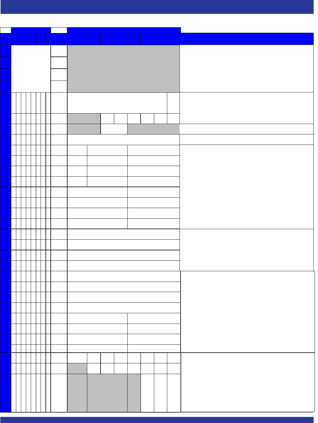
RAM (PROGRAMMING REGISTER) TABLES
ADDR 76543210
Default
Register
Hex Value
7 6543210
BIT #
BIT #
(Default Settings)
DESCRIPTION
0x1F 00000000 00 INV1
0x20 00000000 00 ODIV1_CONFIG0
0x21 00000000 00 ODIV1_CONFIG1
0x22 00000000 00 ODIV1_CONFIG2
0x23 00000000 00 ODIV1_CONFIG3
0x24 00000000 00
0x25 00000000 00
0x26 00000000 00
0x27 00000000 00
0x28 00000000 00
0x29 00000000 00
0x2A 00000000 00
0x2B 00000000 00
0x2C
00000000 00
0x2D 00000000 00
0x2E 00000000 00
0x2F 00000000 00
0x30 00000000 00
0x31 00000000 00
0x32 00000000 00
0x33 00000000 00
0x34 01000110 46 PRIMCLK
0x35
01010101 55
SRC1[1:0] SM[1:0]SRC2[1:0]
OEM1[1;0] SLEW1[1:0]
CP1[3:0]_CONFIG3
A1[3:0]_CONFIG2
N1[7:0]_CONFIG1
N1[7:0]_CONFIG3
D1[7:0]_CONFIG0
N1[11:8]_CONFIG0
CP1[3:0]_CONFIG2
D1[7:0]_CONFIG3
N1[7:0]_CONFIG0
CZ1[3:0]_CONFIG3
D1[7:0]_CONFIG2
CZ1[3:0]_CONFIG2
D1[7:0]_CONFIG1
CP1[3:0]_CONFIG1 CZ1[3:0]_CONFIG1
RZ1[3:0]_CONFIG2
SRC6[1:0] SRC5[1:0] SRC4[1:0]
CP1[3:0]_CONFIG0
IP1[2:0]_CONFIG2
N1[11:8]_CONFIG2
A1[3:0]_CONFIG3 N1[11:8]_CONFIG3
A1[3:0]_CONFIG1 N1[11:8]_CONFIG1
CZ1[3:0]_CONFIG0
RZ1[3:0]_CONFIG0
RZ1[3:0]_CONFIG3
RZ1[3:0]_CONFIG1
SRC3[1:0]
N1[7:0]_CONFIG2
A1[3:0]_CONFIG0
IP1[2:0]_CONFIG0
IP1[2:0]_CONFIG1
IP1[2:0]_CONFIG3
Configuring Output OUT1
INV1=Output Inversion for OUT1 ("0"= Non-Invert (Default), "1"=Invert);
SLEW 1=Slew Rate Settings for OUT1 output ("00"= 2.75V/ns (Default), "01"=2V/ns, "10"=1.25V/ns, "11"=0.7V/ns);
OEM1= Output Enable Mode for OUT1 output, when used with OE1 bit and SHUTDOWN/OE pin ("0x" = Tri-state (Default), "10"=Park
Low, "11"=Park High);
Address 0x1F, Bits 3, 1, 0 are reserved and should be set to "0"
PRIMCLK=Priority Selection for Input Clock ("0"=XTALIN/REF_IN becomes Primary (Default), "1"=CLK_IN becomes Primary);
SM = Switchover Mode ("0x"=Manual, "10"= Auto-NonRevertive, "11"=Auto-Revertive (Default));
Bit 3 is reserved and should be set to "0".
SRCx[1:0]=Input Source Selection for Output Dividers "Qx" blocks ("00"=Selected Input CLK, "01"=PLL0, "10"=PLL1, "11"=PLL2);
Default on SRC1 is the selected input clock. Default on SRC2-6 is PLL0 which will be powered down.
PLL1 LOOP FILTER SETTING
Loop Filter Values for PLL1 - For 4 Configurations (Default value is '0');
CONFIG0 will be selected if GINx are disabled and operating in MFC mode.
ODIV1_CONFIGx=Determines which one of the 2 "Qx-Divider" Configurations to use with, for any of the "Qx-Divider" block associated
with PLL1; Used in MFC mode; Default ODIV value is "0", and use CONFIG0 of Qx-Divider;
Resistor = 0.3KΩ + RZ1[3:0] * 1KΩ, 0.3 to 15.3kOhm with 1kOhm Step, ("0000"=0.3kOhm, "0001"=1.3kOhm, "0010"=2.3kOhm, ...);
Zero capacitor = 6pF + CZ1[3:0] * 27.2pF, 6pF to 414pF with 27.2pF Step, ("0000"=6pF, "0001"=33.2pF, "0010"=60.4pF", ...);
Pole capacitor = 1.3pF + CP1[3:0] * 0.75pF, 1.3pF to 12.55pF with 0.75pF Step, ("0000"=1.3pF, "0001"=2.05pF, "0010"=2.8pF, ...)
Charge pump current = 5 * 2^IP1[2:0] μA, 5uA to 640uA with 5, 10, 20, 40, ... binary step;
PLL1 INPUT DIVIDER D1 SETTING
PLL1 D-Divider Values (Prescaler) - For 4 Configurations (Default value is '0');
PLL1 MULTIPLIER SETTING
CONFIG0 will be selected if GINx are disabled and operating in MFC mode.
N1[11:0]_CONFIGx - Part of PLL1 M Integer Feedback Divider Values (see equation below) - For 4 Configurations (Default value is '0');
A1[3:0]_CONFIGx - Part of PLL1 M Integer Feedback Divider Values (see equation below) - For 4 Configurations (Default value is '0');
SSC_OFFSET1[5:0] - Spread Spectrum Fractional Multiplier Offset Value. See Spread Spectrum Settings in register address range
0x68-0x6F
Total Multiplier Value M1 = 2 * N1[11:0] + A1 + 1 + SS_OFFSET1 * 1/64
When A1[3:0] = 0 and spread spectrum disabled, M1= 2 * N1[11:0];
When A1[3:0] > 0 and spread spectrum disabled, M1 = 2 * N1[11:0] + A1 + 1 ;
(Note: A < N-1, i.e. valid M values are 2, 4, 6, 8, 9, 10, 11, 12, 13, ..., 4095 assuming within fPFD and fVCO spec);
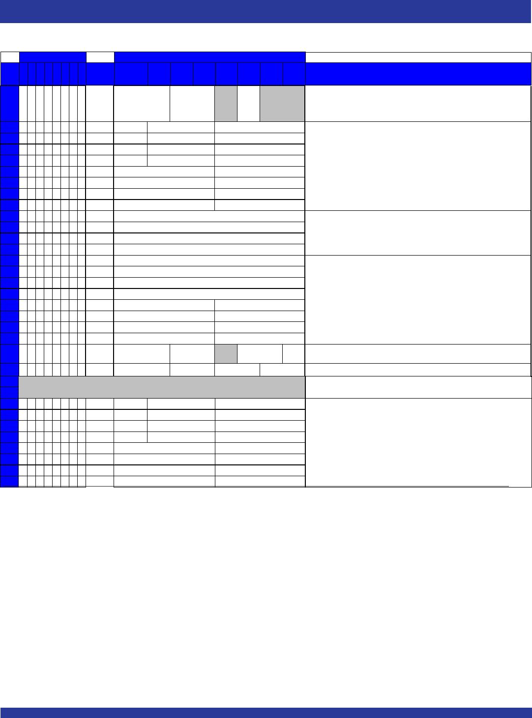
0x36
0x37
0x38 00000000 00 ODIV2_CONFIG0
0x39
00000000 00 ODIV2_CONFIG1
0x3A
00000000 00 ODIV2_CONFIG2
0x3B 00000000 00 ODIV2_CONFIG3
0x3C 00000000 00
0x3D
00000000 00
0x3E 00000000 00
0x3F 00000000 00
CP2[3:0]_CONFIG2
CP2[3:0]_CONFIG1
IP2[2:0]_CONFIG0
RZ2[3:0]_CONFIG1IP2[2:0]_CONFIG1
RZ2[3:0]_CONFIG0
CZ2[3:0]_CONFIG1
IP2[2:0]_CONFIG3
IP2[2:0]_CONFIG2
RZ2[3:0]_CONFIG3
RZ2[3:0]_CONFIG2
CZ2[3:0]_CONFIG0
CZ2[3:0]_CONFIG2
CP2[3:0]_CONFIG0
CP2[3:0]_CONFIG3 CZ2[3:0]_CONFIG3
No Registers Exist
PLL2 LOOP FILTER SETTING
Loop Filter Values for PLL2 - For 4 Configurations (Default value is '0');
CONFIG0 will be selected if GINx are disabled and operating in MFC mode.
ODIV2_CONFIGx=Determines which one of the 2 "Qx-Divider" Configurations to use with, for any of the "Qx-Divider" block associated with
PLL2; Used in MFC mode; Default ODIV value is "0", and use CONFIG0 of Qx-Divider;
Resistor = 0.3KΩ + RZ2[3:0] * 1KΩ, 0.3 to 15.3kOhm with 1kOhm Step, ("0000"=0.3kOhm, "0001"=1.3kOhm, "0010"=2.3kOhm, ...);
Zero capacitor = 6pF + CZ2[3:0] * 27.2pF, 6pF to 414pF with 27.2pF Step, ("0000"=6pF, "0001"=33.2pF, "0010"=60.4pF", ...);
Pole capacitor = 1.3pF + CP2[3:0] * 0.75pF, 1.3pF to 12.55pF with 0.75pF Step, ("0000"=1.3pF, "0001"=2.05pF, "0010"=2.8pF, ...)
Charge pump current = 5 * 2^IP2[2:0] μA, 5uA to 640uA with 5, 10, 20, 40, ... binary step;