13
INDUSTRIAL TEMPERATURE RANGE
IDT5V9885T
3.3V EEPROM PROGRAMMABLE CLOCK GENERATOR
To determine if the loop is stable, the phase margin (ωm) would need to be calculated as follows.
Phase Margin:
ωz = 1 / (Rz * Cz) (Eq. 23)
ωp = Cz + Cp (Eq. 24)
Rz * Cz * Cp
φm = (360 / 2π ) * [tan
-1
(ωc/ ωz) - tan
-1
(ωc/ ωp)] (Eq. 25)
To ensure stability in the loop, the phase margin is recommended to be > 60° but too high will result in the lock time being excessively long. Certain loop filter
parameters would need to be compromised to not only meet a required loop bandwidth but to also maintain loop stability.
Example
Fc = 150KHz is the desired loop bandwidth. The total M value is 850. The ratio of ωp/ωc should be at least 4. A rule of thumb that will help to aid the way,
the ωp / ωc ratio should be at least 4. Given Fc and M, an optimal loop filter setting needs to be solved for that will meet both the PLL loop bandwidth and maintain
loop stability.
The charge pump gain should be relatively small as possible to achieve a low loop bandwidth.
Ip = 40uA .
Kφ * KVCO = 950MHz/V * 40uA = 38000A/Vs
Loop Bandwidths
ωc = 2π * Fc = 9.42x10
5
s
-1
ωuz = ωp / ωc = 4 (Eq. 26)
ωc
2
= ωp * ωz (Eq. 27)
ωp = Cz + Cp = ωz (1 + Cz / Cp)
Rz * Cz * Cp
Solving for Cz, Cp, and Rz
Knowing ωc = Rz * Kφ * KVCO * Cz and substituting in the equations from above,
M * (Cz + Cp)
Cz >>> Cp, therefore, we can easily derive Cp to be
Cp = Kφ * KVCO = 12.60pF
M * ωc
2
* ωuz
Similarly for Cz and Rz
Cz = Kφ * KVCO * (ωuz
2
- 1) = Cp * (ωuz
2
- 1) = 189pF
M * ωc
2
* ωuz
Rz = M * ωc * ωuz
2
= 22.48KΩ
Kφ * KVCO * (ωuz
2
- 1)
Based on the loop filter parameter equations from above, since there are no possible values of 12.60pF for Cp, 189pF for Cz, and 22.48KΩ for Rz, the next
possible values within the loop filter settings are 12.55pF (CP[3:0]=1111), 196.4pF (CZ[3:0]=0111), and 15.3KΩ (RZ[3:0]=1111), respectively. This loop filter
setting will yield a loop bandwidth of about 102KHz. The phase margin must be checked for loop stability.
φm = (360 / 2π ) * [tan
-1
(6.41x10
5
s
-1
/ 3.33x10
5
s
-1
) - tan
-1
(6.41x10
5
s
-1
/ 5.54x10
6
s
-1
)] = 56°
Although slightly below 60°, the phase margin would be acceptable with a fairly stable loop.
14
INDUSTRIAL TEMPERATURE RANGE
IDT5V9885T
3.3V EEPROM PROGRAMMABLE CLOCK GENERATOR
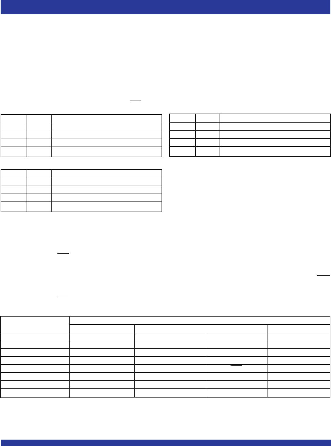
GIN2 Pin GIN1 Pin GIN0 Pin PLL0 Configuration Selection (Mode 1)
0 0 0 Configuration 0
0 0 1 Configuration 1
0 1 0 Configuration 2
0 1 1 Configuration 3
1 0 0 Configuration 4
1 0 1 Configuration 5
1 1 0 Configuration 6
1 1 1 Configuration 7
CONFIGURING THE MULTI-PURPOSE I/Os
The 5V9885T can operate in four distinct modes. These modes are controlled by the MFC bit (0x04) and the I
2
C/JTAG pin. The general purpose I/O pins
(GIN0, GIN1, GIN2, GIN3, GIN4, GIN5) have different uses depending on the mode of operation. The four available modes of operation are:
1) Manual Frequency Control (MFC) Mode for PLL0 Only
2) Manual Frequency Control (MFC) Mode for all three PLLs
3) I
2
C Programming Mode
4) JTAG Programming Mode
Along with the GINx pins are also GOUTx output pins that can take up a different function depending on the mode of operation. See table below for description.
Each PLL's programming registers can store up to four different Dx and Mx configurations in combination with two different P configurations in MFC modes.
The post-divider should never be disabled in any of the two P configurations unless the output bank will never be used during normal operation. The PLL's
loop filter settings also has four different configurations to store and select from. This will be explained in the MODE1 and MODE2 sections. The use of the GINx
pins in MFC mode control the selection of these configurations.
MODE1 - Manual Frequency Control (MFC=1) Mode for PLL0 Only
In this mode, only 8 configurations of PLL0 can be changed during operation. The GIN0, GIN1 and GIN2 pins control the selection of eight different
configurations (D, M, Rz, Cz, Cp and Ip) of PLL0. GIN3 becomes PLL SUSPEND pin, GIN4 is not available to users, and GIN5 becomes CLK_SEL pin.
The output GOUT0 will become an indicator for loss of PLL lock (LOSS_LOCK). GOUT1 pin will become an indicator for loss of the primary clock
(LOSS_CLKIN).
The PLL0 has 4 sets of dedicated registers for D, M, Rz, Cz, Cp, Ip and ODIV. For additional 4 sets of registers, the PLL0 uses registers from CONFIG2
and CONFIG3 of PLL1 and PLL2. The PLL1 and PLL2 will still be fully operational, but have only one fixed configuration in this mode, and the default
configuration will be set to CONFIG0 of PLL1 and CONFIG0 of PLL2. (Please see page 18 for register location.)
The output banks will each have two P configurations that can be associated with each of the PLL configurations. Each of the two P configurations has its
own set of PM bits (See the PRE-SCALERS, FEEDBACK-DIVIDERS, POST-DIVIDERS section for more detail on the PM bits). Use the ODIV bit to
choose which post-divider configuration to associate with a specific PLL configuration.
To enter this mode, users must set MFC bit to “1”, and I2C/JTAG pin must be left floating.
NOTE:
1. Please see detail description in Loss of Lock and Input Clock section.
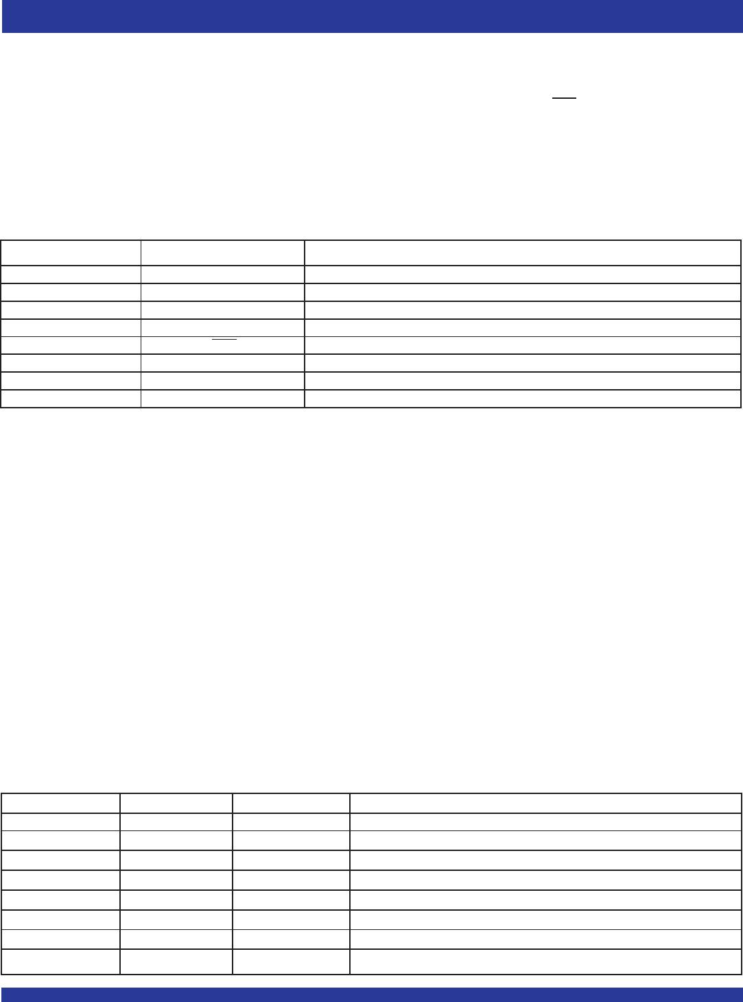
Multi-Purpose Pins Other Signal Functions Signal Description
GIN0 SDAT / TDI I
2
C serial data input / JTAG serial data input
GIN1 SCLK / TCK I
2
C clock input / JTAG clock input
GIN2 TMS JTAG control signal to the TAP controller state machine
GIN3 SUSPEND Suspends all outputs of PLL (Active High)
GIN4 TRST JTAG active LOW input to asynchronously reset the BST
GIN5 CLK_SEL Reference clock select between XTALIN/REFIN and CLKIN
GOUT0 TDO / LOSS_LOCK JTAG serial data output / Detects loss of PLL lock
(1)
GOUT1 LOSS_CLKIN Detects loss of the primary clock source
(1)
15
INDUSTRIAL TEMPERATURE RANGE
IDT5V9885T
3.3V EEPROM PROGRAMMABLE CLOCK GENERATOR
MODE3 - I
2
C Programming Mode
In this mode, GIN0, GIN1, GIN3 and GIN5 become SDAT (I
2
C data), SCLK (I
2
C clock), SUSPEND and CLK_SEL signal pins, respectively. The output GOUT0
will become an indicator for loss of PLL lock (LOSS_LOCK). GOUT1 pin will become an indicator for loss of the primary clock (LOSS_CLKIN). GIN2 and GIN4
are not available to users.
To enter this mode, I
2
C/JTAG pin must be set HIGH.
MODE4 - JTAG Programming Mode
In this mode, GIN0, GIN1, GIN2, GIN3, GIN4 and GIN5 will become TDI (JTAG data in), TCK (JTAG clock), TMS (JTAG control signal), SUSPEND, TRST
(JTAG reset) and CLK_SEL signal pins, respectively. The output GOUT0 will become JTAG TDO signal, and GOUT1 will be an indicator for loss of the selected
clock (LOSS_CLKIN).
To enter this mode, I
2
C/JTAG pin must be set LOW.
MODE2 - Manual Frequency Control (MFC=0) Mode for all PLLs
In this mode, the configuration of PLL0, PLL1, and PLL2 can be changed during operation. The GINx pins are used to control the selection of up to four different
Dx, Mx, RZx, CZx, CPx, and IPx configurations for each PLL. GIN0 and GIN1 become configuration selection pins for D0 and M0 of PLL0, GIN2 and GIN3
become configuration selection pins for PLL1, and GIN4 and GIN5 become configuration selection pins for D2 and M2 of PLL2. The output GOUT0 will become
an indicator for loss of PLL lock (LOSS_LOCK). GOUT1 pin will become an indicator for loss of the primary clock (LOSS_CLKIN).
The output banks will have two different P configurations to choose from for each of the four PLL configurations. Each of the two P configurations has its own
set of PM bits (See the PRE-SCALERS, FEEDBACK-DIVIDERS, POST-DIVIDERS section for more detail on the PM bits). Use the ODIV bit to choose which
post-divider configuration to associate with a specific PLL configuration. For example, if ODIV2_CONFIG2=1, then when Config2 is selected Qx[9:0]_CONFIG1
is selected as the post-divider value to be used. Note that there is an ODIVx bit for each of the PLL configurations. In this way, the post-divider values can change
with the configuration.
To enter this mode, users must set MFC bit to "0", and I
2
C/JTAG pin must be left floating.
GIN1 Pin GIN0 Pin PLL0 Configuration Selection (Mode 2)
0 0 Configuration 0
0 1 Configuration 1
1 0 Configuration 2
1 1 Configuration 3
GIN3 Pin GIN2 Pin PLL1 Configuration Selection (Mode 2)
0 0 Configuration 0
0 1 Configuration 1
1 0 Configuration 2
1 1 Configuration 3
GIN5 Pin GIN4 Pin PLL2 Configuration Selection (Mode 2)
0 0 Configuration 0
0 1 Configuration 1
1 0 Configuration 2
1 1 Configuration 3
Manual Frequency Control modes
Multi-Purpose pins Mode1 Mode2 JTAG I
2
C
GIN0 GIN0 GIN0 TDI SDAT
GIN1 GIN1 GIN1 TCK SCLK
GIN2 GIN2 GIN2 TMS n/a
GIN3 SUSPEND GIN3 SUSPEND SUSPEND
GIN4 n/a GIN4 TRST n/a
GIN5 CLK_SEL GIN5
(1)
CLK_SEL CLK_SEL
GOUT0 LOSS_LOCK LOSS_LOCK TDO LOSS_LOCK
GOUT1 LOSS_CLKIN LOSS_CLKIN LOSS_CLKIN LOSS_CLKIN
NOTE:
1. The PLL(s) will lock onto the primary clock and the manual switchover can be controlled by the PRIMCLK bit.

5V9885TPFGI8

Mfr. #:
Manufacturer:
IDT
Description:
Clock Generators & Support Products SPREAD SPECTRUM PROG . CLK
Lifecycle:
New from this manufacturer.
Delivery:
DHL FedEx Ups TNT EMS
Payment:
T/T Paypal Visa MoneyGram Western Union

Products related to this Datasheet