28
INDUSTRIAL TEMPERATURE RANGE
IDT5V9885T
3.3V EEPROM PROGRAMMABLE CLOCK GENERATOR
POWER SUPPLY CHARACTERISTICS FOR LVTTL OUTPUTS
Symbol Parameter Test Conditions Typ. Max Unit
I
DDQ Quiescent VDD Power Supply Current REF = LOW 6 12 mA
Outputs enabled, All outputs unloaded
I
DDD Dynamic VDD Power Supply VDD = Max., CL = 0pF 40 60 μA/MHz
Current per Output
F
REFERENCE CLOCK = 33MHz, CL = 15pf 26 40
I
TOT Total Power VDD Supply Current FREFERENCE CLOCK = 133MHz, CL = 15pf 80 120 mA
F
REFERENCE CLOCK = 200MHz, CL = 15pf 112 170
NOTES:
1. These inputs are normally wired to V
DD, GND, or left floating. If these inputs are switched dynamically after powerup, the function and timing of the outputs may be glitched, and
the PLL may require additional t
AQ time before all datasheet limits are achieved.
2. Dividers must reload reprogrammed values via power-on reset or terminal count reload in order to ensure low-power mode.
DC ELECTRICAL CHARACTERISTICS OVER OPERATING RANGE
Symbol Parameter Test Conditions Min. Typ. Max. Unit
VIHH Input HIGH Voltage Level
(1)
I
2
C/JTAG 3-Level Input VDD – 0.4 V
VIMM Input MID Voltage Level
(1)
I
2
C/JTAG 3-Level Input VDD/2 – 0.2 VDD/2 + 0.2 V
VILL Input LOW Voltage Level
(1)
I
2
C/JTAG 3-Level Input 0.4 V
V
IN = VDD HIGH Level 200
I
3 3-Level Input DC Current VIN = VDD/2 MID Level 50 +50 μA
VIN = GND LOW Level –200
I
DD Total Power Supply Current 2 outputs @166MHz; 4 outputs @ 83MHz 120 mA
(3.3V Supply, VDD) 2 outputs @20MHz; 4 outputs @ 40MHz 40
I
DDS Total Power Supply Current in Global Shutdown Mode 2 mA
Shutdown Mode
(2)
(PLLs, dividers, outputs, etc. powered down)
DC ELECTRICAL CHARACTERISTICS FOR 3.3V LVTTL
(1)
Symbol Parameter Test Conditions Min. Typ. Max. Unit
IOH Output HIGH Current VOH = VDD - 0.5, VDD = 3.3V ± 0.3V 12 24 mA
IOL Output LOW Current VOL = 0.5V, VDD = 3.3V ± 0.3V 12 24 mA
VIH Input Voltage HIGH 2 V
VIL Input Voltage LOW 0.8 V
IIH Input HIGH Current
(2
)VIN = VDD ——10 μA
IIL Input LOW Current VIN = 0V 10 μA
I
OZD Output Leakage Current 3-state outputs 10 μA
NOTES:
1. See RECOMMENDED OPERATING RANGE table.
2. IIH specification does not apply to inputs with internal pull-down.
29
INDUSTRIAL TEMPERATURE RANGE
IDT5V9885T
3.3V EEPROM PROGRAMMABLE CLOCK GENERATOR
DC ELECTRICAL CHARACTERISTICS FOR LVDS
Symbol Parameter Min. Typ. Max Unit
VOT (+) Differential Output Voltage for the TRUE binary state 247 454 mV
VOT (-) Differential Output Voltage for the FALSE binary state -247 -454 mV
Δ VOT Change in VOT between Complimentary Output States 50 mV
VOS Output Common Mode Voltage (Offset Voltage) 1.125 1.2 1.375 V
Δ VOS Change in VOS between Complimentary Output States 50 mV
IOS Outputs Short Circuit Current, VOUT+ or VOUT- = 0V or VDD —924mA
I
OSD Differential Outputs Short Circuit Current, VOUT+ = VOUT-—612mA
POWER SUPPLY CHARACTERISTICS FOR LVDS OUTPUTS
(1)
Symbol Parameter Test Conditions
(2)
Typ. Max Unit
I
DDQ Quiescent VDD Power Supply Current REF = LOW 68 90 mA
Outputs enabled, All outputs unloaded
I
DDD Dynamic VDD Power Supply VDD = Max., CL = 0pF 30 45 μA/MHz
Current per Output
F
REFERENCE CLOCK = 100MHz, CL = 5pf 86 130
I
TOT Total Power VDD Supply Current FREFERENCE CLOCK = 200MHz, CL = 5pf 100 150 mA
F
REFERENCE CLOCK = 400MHz, CL = 5pf 122 190
POWER SUPPLY CHARACTERISTICS FOR LVPECL OUTPUTS
(1)
Symbol Parameter Test Conditions
(2)
Typ. Max Unit
I
DDQ Quiescent VDD Power Supply Current REF = LOW 86 110 mA
Outputs enabled, All outputs unloaded
I
DDD Dynamic VDD Power Supply VDD = Max., CL = 0pF 35 50 μA/MHz
Current per Output
F
REFERENCE CLOCK = 100MHz, CL = 5pf 120 180
ITOT Total Power VDD Supply Current FREFERENCE CLOCK = 200MHz, CL = 5pf 130 190 mA
F
REFERENCE CLOCK = 400MHz, CL = 5pf 140 210
DC ELECTRICAL CHARACTERISTICS FOR LVPECL
Symbol Parameter Min. Typ. Max Unit
VOH Output Voltage HIGH, terminated through 50Ω tied to VDD - 2V VDD - 1.2 VDD - 0.9 V
VOL Output Voltage LOW, terminated through 50Ω tied to VDD - 2V VDD - 1.95 VDD - 1.61 V
V
SWING Peak to Peak Output Voltage Swing 0.55 0.93 V
NOTES:
1. Output banks 4 and 5 are toggling. Other output banks are powered down.
2. The termination resistors are excluded from these measurements.
NOTES:
1. Output banks 4 and 5 are toggling. Other output banks are powered down.
2. The termination resistors are excluded from these measurements.
30
INDUSTRIAL TEMPERATURE RANGE
IDT5V9885T
3.3V EEPROM PROGRAMMABLE CLOCK GENERATOR
AC TIMING ELECTRICAL CHARACTERISTICS
(SPREAD SPECTRUM GENERATION = OFF)
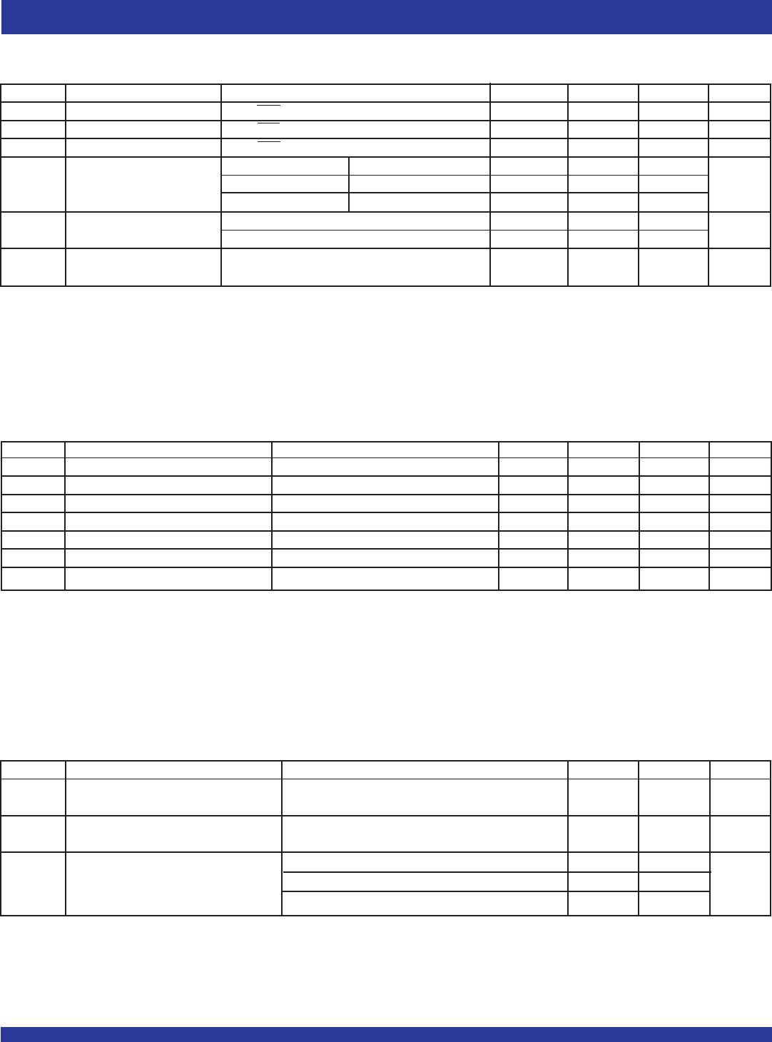
Symbol Parameter Test Conditions Min. Typ. Max Unit
fIN Input Frequency Input Frequency Limit 1
(1)
400 MH z
1/t1 Output Frequency Single Ended Clock output limit (LVTTL) 0.0049 200 MHz
Differential Clock output limit (LVPECL/ LVDS) 0.0049 500
fVCO VCO Frequency VCO operating Frequency Range 10 1200 MHz
fPFD PFD Frequency PFD operating Frequency Range 0.4
(1)
400 MH z
fBW Loop Bandwidth Based on loop filter resistor and capacitor values 0.03 40 MHz
t2 Input Duty Cycle Duty Cycle for Input 40 60 %
t3 Output Duty Cycle Measured at V
DD/2, FOUT 200MHz 45 55 %
Measured at VDD/2, FOUT > 200MHz 40 60
Slew Rate Single-Ended Output clock rise and fall time, 2.75
SLEWx(bits) = 00 20% to 80% of V
DD (Output Load = 15pf)
Slew Rate Single-Ended Output clock rise and fall time, 2
t4
(2)
SLEWx(bits) = 01 20% to 80% of VDD (Output Load = 15pf) V/ns
Slew Rate Single-Ended Output clock rise and fall time, 1.25
SLEWx(bits) = 10 20% to 80% of VDD (Output Load = 15pf)
Slew Rate Single-Ended Output clock rise and fall time, 0.75
SLEWx(bits) = 11 20% to 80% of VDD (Output Load = 15pf)
Rise Times LVDS, 20% to 80% 850
t5 Fall Times 850 ps
Rise Times LVPECL, 20% to 80% 500
Fall Times 500
t6 Output three-state Timing Time for output to enter or leave three-state mode 150 + ns
after SHUTDOWN/OE switches 1/FOUTX
t7 Clock Jitter
(3,7)
Peak-to-peak period jitter, fPFD > 20MHz 150 ps
CLK outputs measured at VDD/2 fPFD < 20MHz 200
t8 Output Skew Skew between output to output on the same bank 150 ps
(bank 4 and bank 5 only)
(4, 5)
t9 Lock Time PLL Lock Time from Power-up
(6)
—1020ms
t10 Lock time
(8)
PLL Lock time from shutdown mode 20 100 μs
NOTES:
1. Practical lower input frequency is determined by loop filter settings.
2. A slew rate of 2V/ns or greater should be selected for output frequencies of 100MHz and higher.
3. Input frequency is the same as the output with all output banks running at the same frequency.
4. Skew measured between all in-phase outputs in the same bank.
5. Skew measured between the cross points of all differential output pairs under identical input and output interfaces, transitions and load conditions on any one device.
6. Includes loading the configuration bits from EEPROM to PLL registers. It does not include EEPROM programming/write time.
7. Guaranteed by design but not production tested. Actual jitter performance may vary depending on the configuration.
8. Actual PLL lock time depends on the loop configuration.
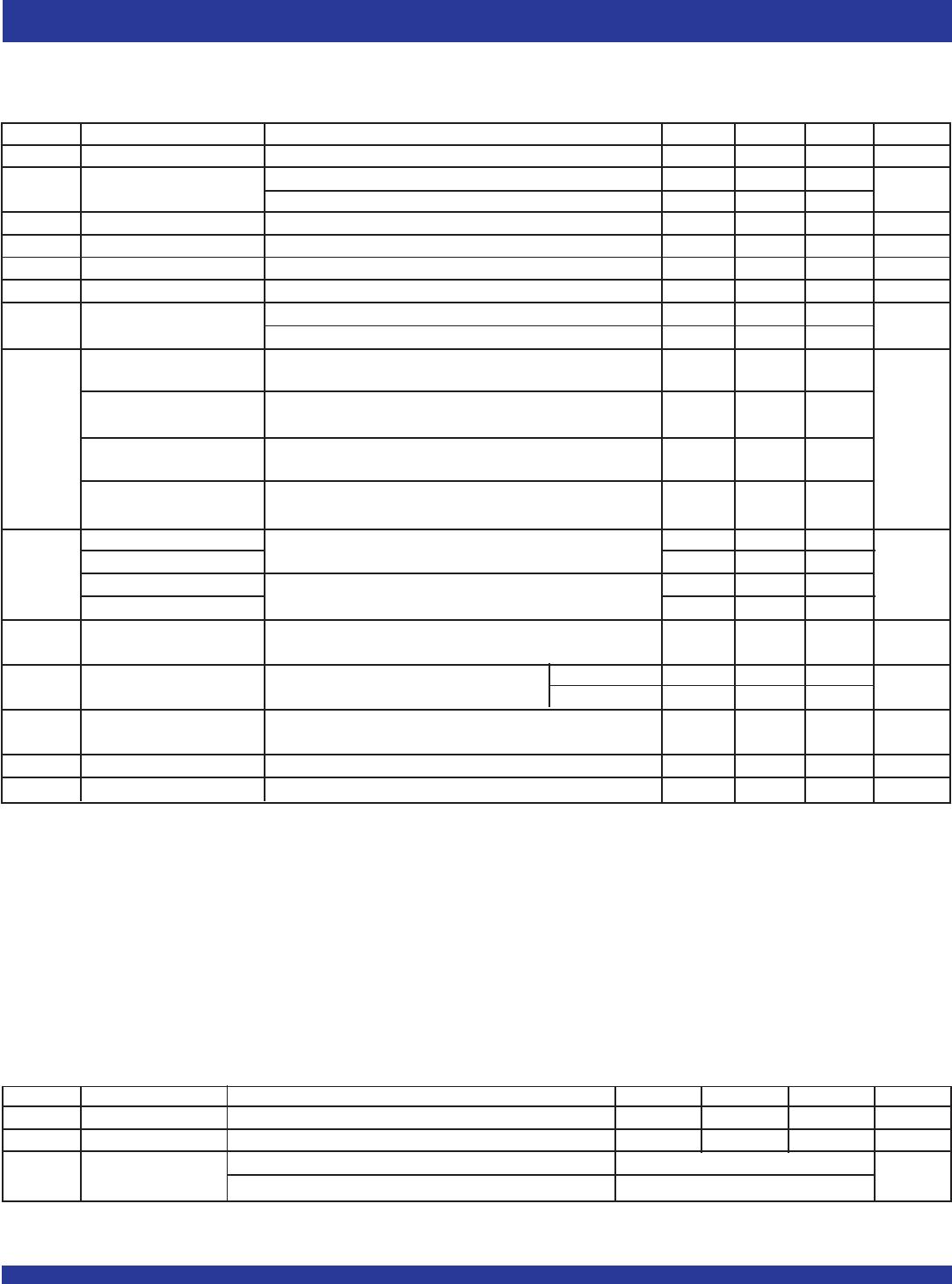
SPREAD SPECTRUM GENERATION SPECIFICATIONS
Symbol Parameter Description Min. Typ. Max Unit
fIN Input Frequency Input Frequency Limit 1
(1)
400 MHz
fMOD Mod Freq Modulation Frequency 33 k Hz
f
SPREAD Spread Value Amount of Spread Value (Programmable) - Down Spread -0.5, -1, -2.5, -3.5, -4 %fOUT
Amount of Spread Value (Programmable) - Center Spread -2.0 to +2.0
NOTE:
1. Practical lower input frequency is determined by loop filter settings.

5V9885TPFGI8

Mfr. #:
Manufacturer:
IDT
Description:
Clock Generators & Support Products SPREAD SPECTRUM PROG . CLK
Lifecycle:
New from this manufacturer.
Delivery:
DHL FedEx Ups TNT EMS
Payment:
T/T Paypal Visa MoneyGram Western Union

Products related to this Datasheet