16
INDUSTRIAL TEMPERATURE RANGE
IDT5V9885T
3.3V EEPROM PROGRAMMABLE CLOCK GENERATOR
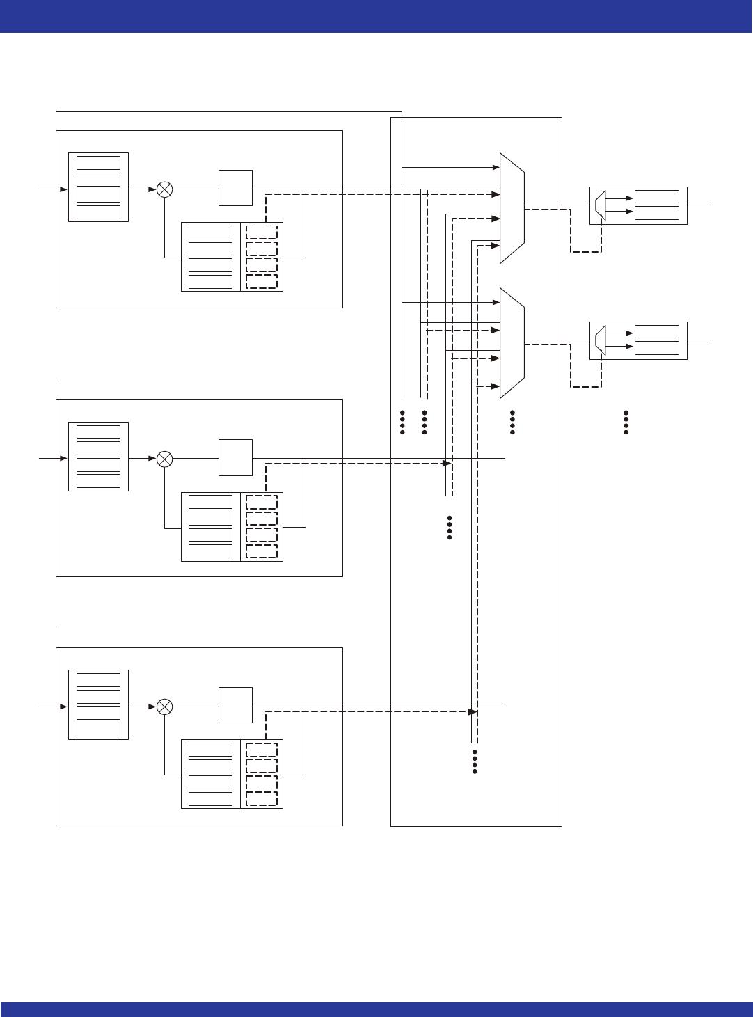
Understanding the GIN Signals
During power up, the part will virtually be in MFC mode2, therefore, the values of GIN4, GIN3, GIN2, GIN1 and GIN0 will be latched and used for PLL
configuration selection, regardless of the state of the I
2
C/JTAG pin. GIN5 is not latched, and will assume the LOW state internally when in programming mode.
This means that when in programming mode, the PLL configuration can only be changed by writing directly to the registers of the currently selected configuration.
When in MFC mode 2, configuration 0 or 1 (GIN5=0) should be selected if you do not want to change configurations when entering or leaving programming
mode. The GIN pins should be held LOW during power up to select configuration0 as default.
When not in programming mode, the GIN inputs directly control the selected configuration. The internal GINx signals can be individually disabled via
programming the GINEN bits (0x06). When disabled by setting GINENx to "0", the GINx inputs may be left floating, but during power up, the GIN pins will still
latch. Disabled inputs are interpreted as LOW by the internal state machines. Even if disabled, GIN2, GIN1, GIN0 and GIN4 pins will be enabled if required
for I
2
C or JTAG programming functions when in programming mode. The SUSPEND and CLK_SEL functions on the GIN3 and GIN5 pins, respectively, will
be rendered completely non-functional when disabled.
SHUTDOWN/SUSPEND/ENABLE OF OUTPUTS
There are two external pins along with internal bits that control the enabling/disabling of the output banks. The two pins are the SHUTDOWN/OE pin and
the GIN3/SUSPEND pin. The SHUTDOWN/OE pin can be programmed to function as an output enable or global shutdown. The polarity of the SHUTDOWN/
OE signal pin can be programmed to be either active HIGH or LOW with the SP bit (0x1C). When SP is "0", the pin becomes active HIGH and when SP is
"1", the pin becomes active LOW. The SH bit(0x1C) determines the function of the SHUTDOWN/OE signal pin. If SH is "1", the signal pin is SHUTDOWN
and functions as a global shutdown. This will override the OEx (0x1C), OSx (0x1D), and PLLSx (0x1E) bits. If SH is "0", the signal pin is OE and functions
as an enable/disable of the output banks. If used as an output enable/disable, each output bank can be individually programmed to be enabled or disabled
by the OE pin.by setting OEx bits to "1". If the OE signal pin is asserted, the output banks that has their corresponding OEx bit set to "1" will be disabled. The
OEMx bits determine the outputs' disable state. When set to "0x" the outputs will be tristated. When set to "10", the outputs will be pulled low. When set to "11",
the outputs will be pulled high. Inverted outputs will be parked in the opposite state. If the OEx bits are set to "0", the states of the corresponding output banks
will not be impacted by the state of the OE pin. To individually enable/disable via programming instead of the OE pin, hard wire the OE pin to Vdd or GND (depending
if it is active HIGH or LOW) as if to disable the outputs. Then toggle the OEx bits to either "0" to enable or "1" to disable.
When the chip is in shutdown, the outputs, the reference oscillator, and the I
2
C /JTAG pin are powered down. The outputs will be tristated and the I
2
C
/JTAG pin will be set to MFC mode (MID level). Programming will not be allowed. The GINx pins and clock inputs remain operational. The PLL is not disabled.
The SHUTDOWN pin must be reasserted in order to program the part or to resume operation.
The GIN3/SUSPEND pin, when used as a SUSPEND function, can be used to power down the PLL and/or output banks.. Each output bank can be
individually programmed to be enabled or disabled by the SUSPEND signal pin by setting the OSx bits to "1". If the SUSPEND signal pin is asserted, the output
banks that has their corresponding OSx bit set to "1" will be powered down and outputs tristated. If the OSx bits are set to "0", the states of the corresponding
output banks will not be impacted by the state of the SUSPEND pin. There is also an option to suspend individual PLLs by setting the PLLSx bits (0x1E) to
"1". This will associate the PLL to the SUSPEND pin. When the pin is asserted, the corresponding PLLs will be powered down. It will not only power down
the PLL but also any output bank associated with it. The PLLSx bits will override the OSx bits.
In the event of a PLL suspend, the PLL must achieve lock again after it has been re-enabled, In the event of a global shutdown, the PLL does not have
to re-acquire lock since it is not disabled.