WM8737L Production Data
w
PD, Rev 4.4, January 2012
10
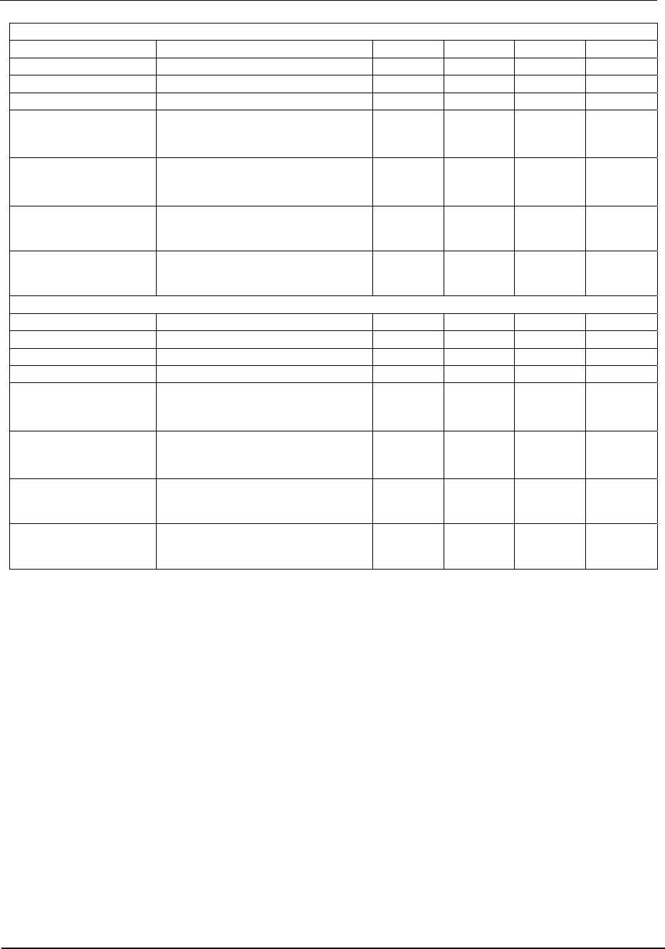
MVDD = 1.8V, AVDD = 1.8V, DBVDD = 1.8V, DCVDD = 1.5V, Normal Power Mode, no MICBIAS or mic preamps
OFF 000000000
0.000 0.000 0.007 0.011
Standby 110000000
0.698 0.004 0.069 1.367
Mono (L/R) 111101000 / 111010100
3.453 0.010 1.910 9.098
Stereo / Digital Mono Mix 111111100
6.109 0.017 1.955 13.959
Analogue mono mix
(without dc monitoring via
Right ADC)
111111000
4.574 0.010 1.910 11.116
Analogue mono mix
(with continuous dc
monitoring via Right ADC)
111111100
6.109 0.017 1.940 13.937
Using MICBIAS in 0.9 X
AVDD mode in addition to
any of the above
Set appropriate MICBIAS[1:0] bits in
power management register
+0.252 - - +0.454
Using microphone boost
preamplifiers in addition to
any of the above
Set appropriate MBCTRL[1:0] bits in
register 09h and set LMBE and/or RMBE
bits in registers 02h and 03h
+0.738 - - +1.328
MVDD = 3.3V, AVDD = 3.3V, DBVDD = 3.3V, DCVDD = 1.5V, Normal Power Mode, no MICBIAS or mic preamps
OFF 000000000
0.001 0.000 0.007 0.014
Standby 110000000
1.288 0.007 0.064 4.371
Mono (L/R) 111101000 / 111010100
4.632 0.020 1.905 18.210
Stereo / Digital Mono Mix 111111100
7.750 0.032 1.950 28.606
Analogue mono mix
(without dc monitoring via
Right ADC)
111111000
5.996 0.020 1.890 22.688
Analogue mono mix
(with continuous dc
monitoring via Right ADC)
111111100
7.750 0.033 1.960 28.624
Using MICBIAS in 0.9 X
AVDD mode in addition to
any of the above
Set appropriate MICBIAS[1:0] bits in
power management register
+0.446 - - +1.472
Using microphone boost
preamplifiers in addition to
any of the above
Set appropriate MBCTRL[1:0] bits in
register 09h and set LMBE and/or RMBE
bits in registers 02h and 03h
+1.406 - - +4.640
Table 1 Supply Current Consumption (see also “Power Management” section)
Notes:
1. T
A
= +25
o
C, Slave Mode, fs = 48kHz, MCLK = 12.288 MHz (256fs), 24-bit data
2. All figures are quiescent, with no signal.
Production Data WM8737L
w
PD, Rev 4.4, January 2012
11
SIGNAL TIMING REQUIREMENTS
SYSTEM CLOCK TIMING
MCLK
t
MCLKL
t
MCLKH
t
MCLKY
Figure 1 System Clock Timing Requirements
Test Conditions
DBVDD = 3.3V, DCVDD = 1.42 to 3.6V, DGND = 0V, T
A
= +25
o
C, Slave Mode fs = 48kHz, MCLK = 256fs, 24-bit data, unless
otherwise stated.
PARAMETER SYMBOL MIN TYP MAX UNIT
System Clock Timing Information
MCLK System clock pulse width high
T
MCLKL
13 ns
MCLK System clock pulse width low
T
MCLKH
13 ns
MCLK System clock cycle time
T
MCLKY
26 ns
AUDIO INTERFACE TIMING – MASTER MODE
BCLK
(Output)
ADCDAT
ADCLRC
(Output)
t
DL
t
DDA
Figure 2 Digital Audio Data Timing – Master Mode (see Control Interface)
Test Conditions
DBVDD = 3.3V, DCVDD = 1.42 to 3.6V, DGND = 0V, T
A
= +25
o
C, Slave Mode, fs = 48kHz, MCLK = 256fs, 24-bit data, unless
otherwise stated.
PARAMETER SYMBOL MIN TYP MAX UNIT
Audio Data Input Timing Information
ADCLRC propagation delay from BCLK falling edge
t
DL
0 10 ns
ADCDAT propagation delay from BCLK falling edge
t
DDA
0 10 ns
AUDIO INTERFACE TIMING – SLAVE MODE
BCLK
ADCLRC
t
BCH
t
BCL
t
BCY
ADCDAT
t
LRSU
t
LRH
t
DD
Figure 3 Digital Audio Data Timing – Slave Mode
WM8737L Production Data
w
PD, Rev 4.4, January 2012
12
Test Conditions
DBVDD = 3.3V, DCVDD = 1.42 to 3.6V, DGND = 0V, T
A
= +25
o
C, Slave Mode, fs = 48kHz, MCLK = 256fs, 24-bit data, unless
otherwise stated.
PARAMETER SYMBOL MIN TYP MAX UNIT
Audio Data Input Timing Information
BCLK cycle time
t
BCY
50 ns
BCLK pulse width high
t
BCH
20 ns
BCLK pulse width low
t
BCL
20 ns
ADCLRC set-up time to BCLK rising edge
t
LRSU
10 ns
ADCLRC hold time from BCLK rising edge
t
LRH
10 ns
ADCDAT propagation delay from BCLK falling edge
t
DD
0 10 ns
CONTROL INTERFACE TIMING – 3-WIRE MODE
CSB
SCLK
SDIN
t
CSL
t
DHO
t
DSU
t
CSH
t
SCY
t
SCH
t
SCL
t
SCS
LSB
t
CSS
Figure 4 Control Interface Timing – 3-Wire Serial Control Mode
Test Conditions
DBVDD = 3.3V, DCVDD = 1.42 to 3.6V, DGND = 0V, T
A
= +25
o
C, Slave Mode, fs = 48kHz, MCLK = 256fs, 24-bit data, unless
otherwise stated.
PARAMETER SYMBOL MIN TYP MAX UNIT
Program Register Input Information
SCLK rising edge to CSB rising edge
t
SCS
40 ns
SCLK pulse cycle time
t
SCY
80 ns
SCLK pulse width low
t
SCL
40 ns
SCLK pulse width high
t
SCH
40 ns
SDIN to SCLK set-up time
t
DSU
10 ns
SCLK to SDIN hold time
t
DHO
10 ns
CSB pulse width low
t
CSL
10 ns
CSB pulse width high
t
CSH
10 ns
CSB rising to SCLK rising
t
CSS
10 ns
Pulse width of spikes which will be suppressed
t
SP
0 5 ns
CONTROL INTERFACE TIMING – 2-WIRE MODE
SDIN
SCLK
t
3
t
1
t
6
t
2
t
7
t
5
t
4
t
3
t
8
t
9
Figure 5 Control Interface Timing – 2-Wire Serial Control Mode

WM8737CLGEFL/R

Mfr. #:
Manufacturer:
Cirrus Logic
Description:
Audio A/D Converter ICs Stereo ADC Low Power
Lifecycle:
New from this manufacturer.
Delivery:
DHL FedEx Ups TNT EMS
Payment:
T/T Paypal Visa MoneyGram Western Union

Products related to this Datasheet