Production Data WM8737L
w
PD, Rev 4.4, January 2012
29
The clocking of the WM8737L is controlled using the CLKDIV2, USB, and SR control bits. Setting the
CLKDIV2 bit divides MCLK by two internally. The USB bit selects between ‘Normal’ and USB mode.
Each combination of the SR4 to SR0 control bits selects one sample rate (see next page). The digital
filter characteristics are automatically adjusted to suit the MCLK and sample rate selected (see Digital
Filter Characteristics).
Since all sample rates are generated by dividing MCLK, their accuracy depends on the accuracy of
MCLK. If MCLK changes, the sample rates change proportionately. Note that some sample rates (e.g.
44.1kHz in USB mode) are approximated, i.e. they differ from their target value by a very small
amount. This is not audible, as the maximum deviation is only 0.27% (48.0214kHz instead of 48kHz
in USB mode - for comparison, a half-tone step corresponds to a 5.9% change in pitch).
In slave mode, it is possible to autodetect the audio clock rate ratio, instead of programming it. The
WM8737L can autodetect the following clock ratios:
CLKDIV2 = 0: MCLK = 128f
s
, 192f
s
, 256f
s
, or 384f
s
subject to MCLK < 40MHz
CLKDIV2 = 1: MCLK = 256f
s
, 384f
s
, 512f
s
, 768f
s
, 1024f
s
, 1536f
s
, subject to MCLK <
40MHz
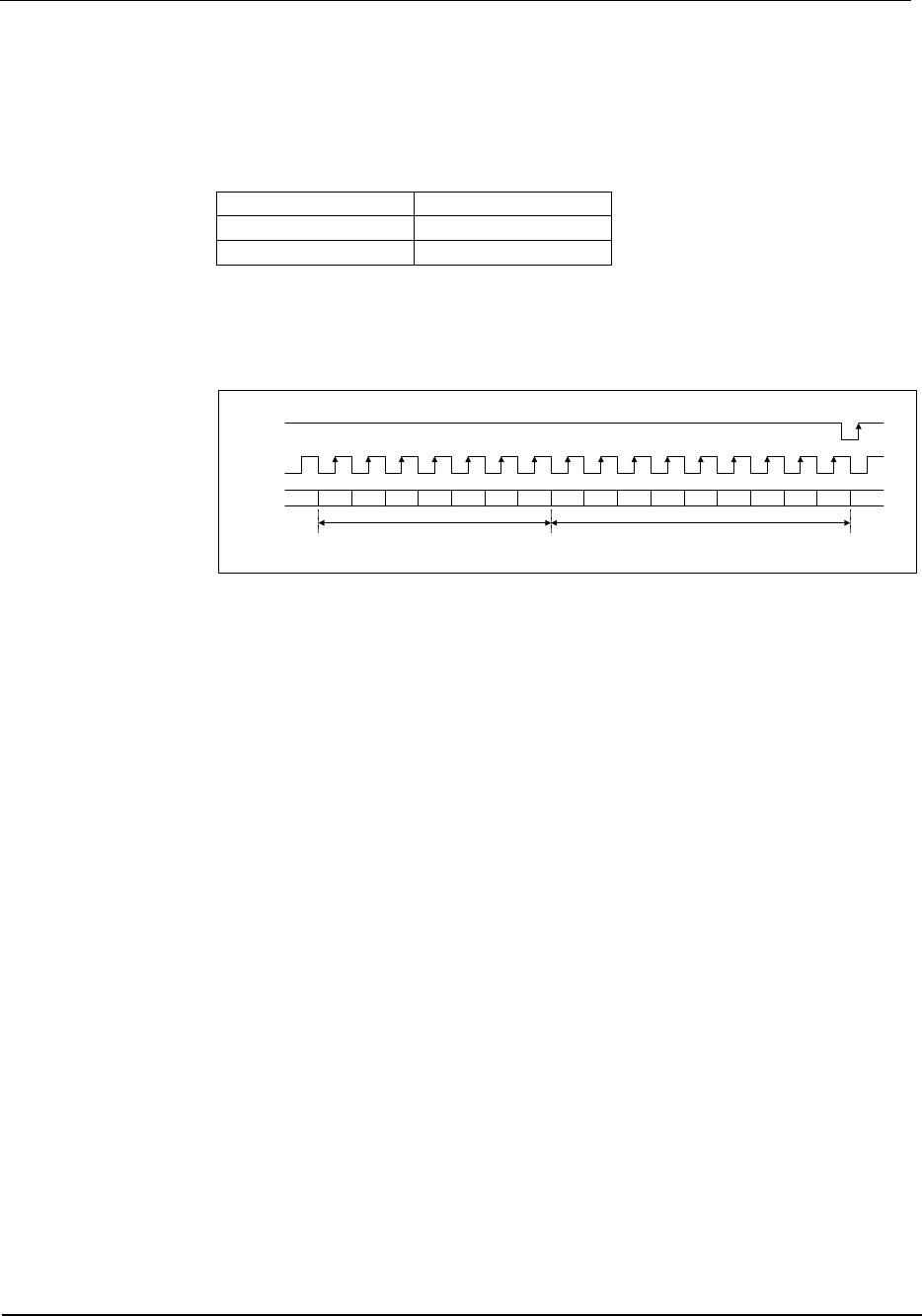
MCLK
CLKDIV2=0
MCLK
CLKDIV2=1
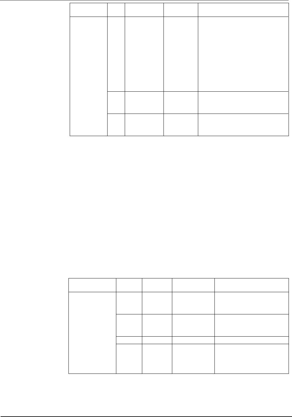
ADC SAMPLE RATE USB SR [4:0] FILTER
TYPE
Normal Clock Mode
12.288MHz 24.576MHz 16 kHz (MCLK/768) 0 01010 A
24 kHz (MCLK/512) 0 11100 A
32 kHz (MCLK/384) 0 01100 A
48 kHz (MCLK/256) 0 00000 A
96 kHz (MCLK/128) (see Note 1) 0 01110 B
11.2896MHz
22.5792MHz
22.05 kHz (MCLK/512) 0 11010 A
44.1 kHz (MCLK/256) 0 10000 A
88.2 kHz (MCLK/128) (see Note 1) 0 11110 B
18.432MHz
36.864MHz
16 kHz (MCLK/1152) 0 01011 A
24 kHz (MCLK/768) 0 11101 A
32 kHz (MCLK/576) 0 01101 A
48 kHz (MCLK/384) 0 00001 A
96 kHz (MCLK/192) (see Note 1) 0 01111 B
16.9344MHz
33.8688MHz
22.05 kHz (MCLK/768) 0 11011 A
44.1 kHz (MCLK/384) 0 10001 A
88.2 kHz (MCLK/192) (see Note 1) 0 11111 B
USB Mode
12.000MHz 24.000MHz 16 kHz (MCLK/750) 1 01010 C
22.0588 kHz (MCLK/544) 1 11011 A
24 kHz (MCLK/500) 1 11100 C
32 kHz (MCLK/375) 1 01100 C
44.118 kHz (MCLK/272) 1 10001 A
48 kHz (MCLK/250) 1 00000 C
88.235 kHz (MCLK/136) (see Note 1) 1 11111 B
96 kHz (MCLK/125) 1 01110 D
Table 16 Master Clock and Sample Rates
Note 1: The 3D enhancement is not supported at sample frequencies of 88.2kHz, 88.235kHz,
and 96kHz. When using these sample frequencies the 3D enhancement function
should be bypassed by first setting register R13 (0Dh) to 1_110x_xxxx (1C0h), where
x_xxxx represents the required values for the ALC in the application, and then setting
register R28 (1Ch) to 0_0000_0100 (004h).
Note that the above sequence uses test bits that are not documented and the use of
these test bits, other than as described above, is not recommended and is not
supported.