WM8737L Production Data
w
PD, Rev 4.4, January 2012
8
Test Conditions
DCVDD = 1.5V, AVDD = MVDD = 3.3V, T
A
= +25
o
C, 1kHz -1dBFS signal, Normal Power Mode, fs = 48kHz, PGA gain = 0dB, 24-
bit audio data, unless otherwise stated.
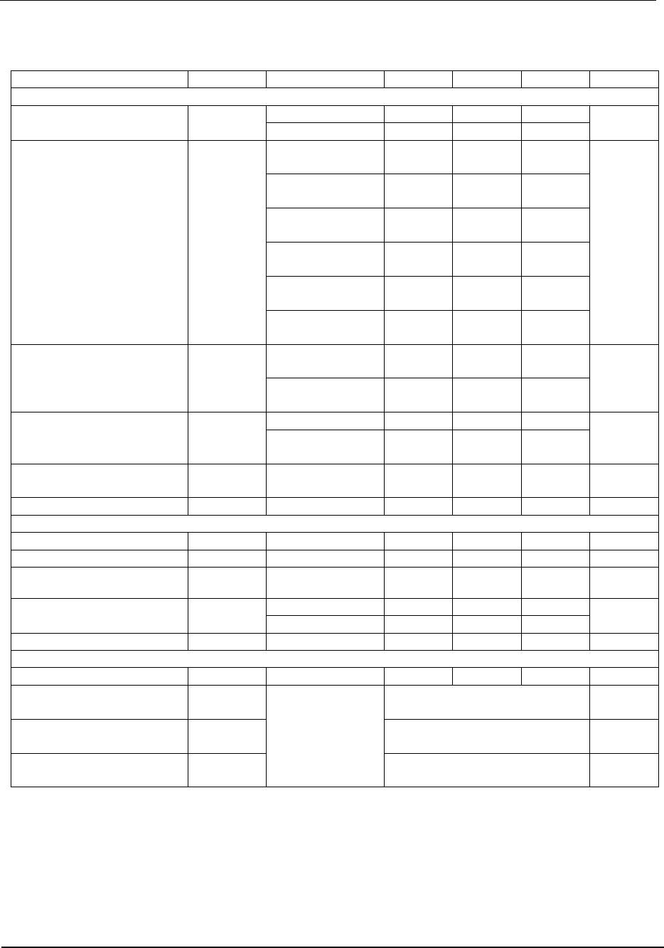
PARAMETER SYMBOL TEST CONDITIONS MIN TYP MAX UNIT
Analogue Reference Levels
Mid-rail Reference Voltage VMID
–3% AVDD/2 +3% V
VMID Output Resistance R
VMID
75 k
Buffered Reference Voltage VREF
–3% AVDD/2 +3% V
Microphone Bias
Bias Voltage
V
MICBIAS
MICBIAS = 01 0.75AVDD V
MICBIAS = 10 0.9AVDD
–3%
0.9AVDD 0.9AVDD
+3%
V
MICBIAS = 11,
AVDD = 2.5V
1.2AVDD V
Bias Current Source
I
MICBIAS
3 mA
Output Noise Voltage
Vn 1K to 20kHz 24 nV/Hz
Digital Input / Output
Input HIGH Level
V
IH
0.7DBVDD V
Input LOW Level
V
IL
0.3DBVDD V
Output HIGH Level
V
OH
I
OH
= 1mA 0.9DBVDD V
Output LOW Level
V
OL
I
OL
= -1mA 0.1DBVDD V
TERMINOLOGY
1. Signal-to-noise ratio (dB) – for the microphone preamplifiers, quoted SNR is the ratio of the rms voltages of the full-
scale output at the L/RACOUT pins and the noise observed at these pins with no input signals. This figure indicates
only the microphone preamplifier noise and does not account for additional noise that will be added by the PGAs and
ADCs in obtaining the final digitised result. For the line inputs, quoted SNR is the ratio of the rms code ranges as
measured at the ADC output for a full-scale output signal and the noise observed with no input. This figure combines
the PGA and ADC noise contributions. (No Auto-zero or Auto-mute function is employed in achieving these results).
2. Dynamic range (dB) - DR measures the ratio in the ADC output between the full-scale signal power and all power
contributed by noise and spurious tones in the specified bandwidth. Normally THD+N is measured at 60dB below full
scale (to reduce any distortion components to negligible levels) and the measurement is then corrected by adding the
60dB to its magnitude. (e.g. THD+N @ -60dB= -32dB, DR= 60 + |-32| = 92dB).
3. Total Harmonic Distortion and Noise (dB) - THD+N is a ratio of the rms values of (Noise + Distortion) and Signal.
4. Channel Separation (dB) - Also known as Cross-Talk. This is a measure of the amount one channel is isolated from
the other. Normally measured by sending a full scale signal down one channel and measuring how much of this signal
appears at the output of the other channel.
5. Hold Time is the length of time between a signal detected by the ALC as being too quiet and beginning to ramp up the
gain. It does not apply to ramping down the gain when the signal is too loud, which happens without a delay.
6. Ramp-up and Ramp-Down times are defined as the time it takes for the PGA to sweep across 90% of its gain range.
7. All hold, ramp-up and ramp-down times scale proportionally with MCLK
Notes:
1. All performance measurements are done with a 20kHz low pass filter, and where noted an A-weight filter. Failure to
use such a filter will result in higher THD+N and lower SNR and Dynamic Range readings than are found in the
Electrical Characteristics. The low pass filter removes out of band noise; although this is not audible, it may affect
dynamic specification values.
2. VMID and VREF are each to be decoupled to a clean analogue ground with 10uF and 0.1uF capacitors placed as
close to the device package as possible. Smaller capacitors may reduce performance. VREFP should be connected to
VREF and VREFN should be connected to AGND using short PCB traces. It is not recommended to connect other
components to VMID or VREF in case of noise injection to the internal references of the device.