WM8737L Production Data
w
PD, Rev 4.4, January 2012
4
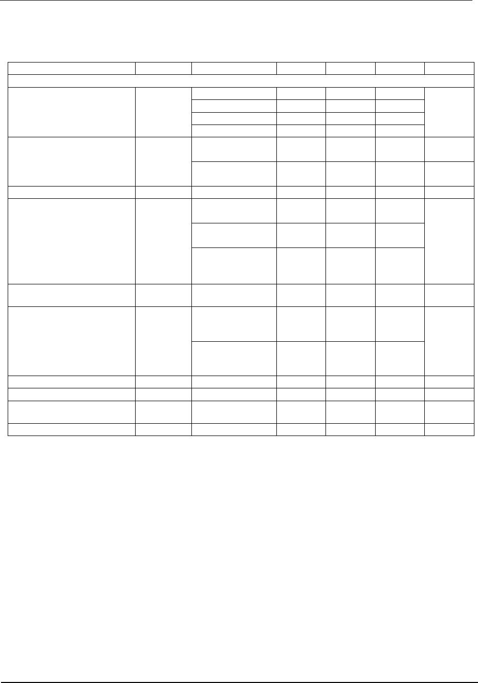
PIN DESCRIPTION
PIN NO NAME TYPE DESCRIPTION
1 NC
No Connect No Internal Connection
2 SCLK
Digital Input Control Interface Clock Input
3 DBVDD
Supply Digital Buffer (I/O) Supply
4 DCVDD
Supply Digital Core Supply
5 DGND
Supply Digital Ground (return path for both DCVDD and DBVDD)
6 NC
No Connect No Internal Connection
7 MCLK
Digital Input Master Clock
8 BCLK
Digital Input / Output Audio Interface Bit Clock
9 ADCDAT
Digital Output ADC Digital Audio Data
10 ADCLRC
Digital Input / Output Audio Interface Left / Right Clock
11 MODE
Digital Input Control Interface Selection
12 AGND
Supply Analogue Ground (return path for both AVDD and MVDD)
13 MICBIAS
Analogue Output Microphone Bias
14 MVDD
Supply Microphone Bias and Microphone Pre-amplifier Positive Supply
15 AVDD
Supply Analogue Positive Supply
16 RACIN
Analogue Input Right Channel DC Blocking Capacitor
17 RACOUT
Analogue Output Right Channel DC Blocking Capacitor
18 RINPUT3
Analogue Input Right Channel Input 3
19 RINPUT2
Analogue Input Right Channel Input 2
20 RINPUT1
Analogue Input Right Channel Input 1
21 LINPUT1
Analogue Input Left Channel Input 1
22 LINPUT2
Analogue Input Left Channel Input 2
23 LINPUT3
Analogue Input Left Channel Input 3
24 LACOUT
Analogue Output Left Channel DC Blocking Capacitor
25 LACIN
Analogue Input Left Channel DC Blocking Capacitor
26 VMID
Analogue Output Midrail Voltage Decoupling Capacitor
27 VREF
Analogue Output Reference Voltage Decoupling Capacitor
28 VREFP
Analogue Output Positive Reference Decoupling Connection
29 VREFN
Analogue Output Negative Reference Decoupling Connection
30 AGND
Supply Analogue Ground (return path for both AVDD and MVDD)
31 CSB
Digital Input Chip Select / Device Address Selection
32 SDIN
Digital Input / Output Control Interface Data Port