Production Data WM8737L
w
PD, Rev 4.4, January 2012
31
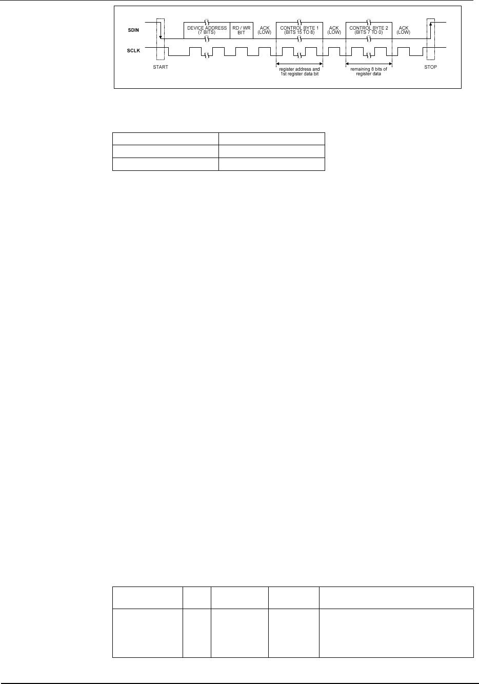
Figure 18 2-Wire Serial Control Interface
The WM8737L has two possible device addresses, which can be selected using the CSB pin.
CSB STATE DEVICE ADDRESS
Low or Unconnected 0011010
High 0011011
Table 18 2-Wire MPU Interface Address Selection
POWER SUPPLIES
The WM8737L can use up to four separate power supplies:
AVDD/AGND: Analogue supply, powers all analogue functions except the microphone pre-amp
and MICBIAS. AVDD can range from 1.8V to 3.6V and has the most significant impact on
overall power consumption. A large AVDD improves audio quality by increasing the maximum
input signal range and thus SNR.
MVDD: Supply pin for microphone pre-amp and MICBIAS only. This separate pin makes it
possible to generate MICBIAS voltages larger than AVDD up to a maximum of 3.6V. If this is
not necessary, MVDD should also be tied to AVDD.
DCVDD: Digital core supply, powers all digital functions except the audio and control interface
pins. DCVDD can range from 1.42V to 3.6V, and has no effect on audio quality. The return path
for DCVDD is DGND, which is shared with DBVDD.
DBVDD: Digital buffer supply, powers the audio and control interface pins. This makes it
possible to run the digital core at very low voltages, saving power, while interfacing to other
digital devices using a higher voltage. DBVDD draws much less power than DCVDD, and has
no effect on audio quality. The return path for DBVDD is DGND, which is shared with DCVDD.
It is possible to use the same supply voltage on all three. However, digital and analogue supplies
should be routed and decoupled separately to keep digital switching noise out of the analogue signal
paths.
POWER MANAGEMENT
The WM8737L has a power management register that allows users to select which functions are
active. For minimum power consumption, unused functions should be disabled. To avoid any pop or
click noise.
When the WM8737L is not in use, it can be put into either one of two standby modes or OFF mode.
OFF mode is achieved by writing zeros to all bits in the power management register and gives lowest
power consumption, but wake-up may take several seconds if the VMID decoupling capacitor has
discharged, as it must be recharged from the selectable impedance VMID source.
The output impedance of VMID can be changed to allow variable voltage stabilization time after VMID
is powered on. The 300kΩ setting will ensure minimum VMID power consumption but with slow
charging time, while the 2.5kΩ setting will allow a more rapid charging time but with the penalty of
greatly increased VMID power consumption. The default 75kΩ setting is recommended for most
applications.
REGISTER
ADDRESS
BIT LABEL DEFAULT DESCRIPTION
R10 (0Ah)
VMID
Impedance
Control
3:2
VMIDSEL 00 VMID impedance selection control
00: 75kΩ output
01: 300kΩ output
10: 2.5kΩ output
Table 19 VMID Impedance Selection