LTC6803-2/LTC6803-4
10
680324fa
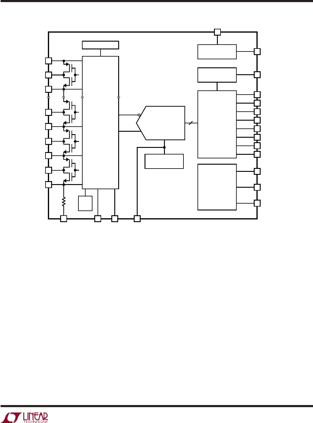
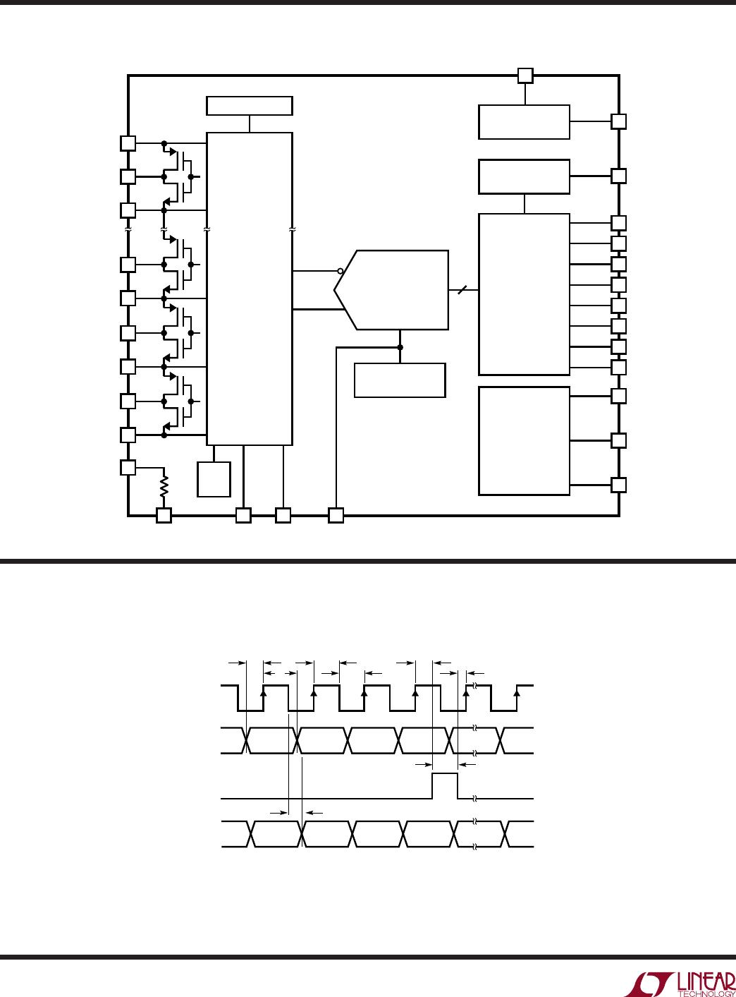
PIN FUNCTIONS
WDTB (Pin 34): Watchdog Timer Output (Active Low). If
there is no valid command received in 1 to 2.5 seconds, the
WDTB output is asserted. The WDTB pin is an open-drain
NMOS output. When asserted it pulls the output down to
V
–
and resets the configuration register to its default state.
GPIO1, GPIO2 (Pins 35, 36): General Purpose Input/
Output. By writing a “0” to a GPIO configuration register
bit, the open-drain output is activated and the pin is pulled
to V
–
. By writing a logic “1” to the configuration register
bit, the corresponding GPIO pin is high impedance. An
external resistor is required to pull the pin up to V
REG
.
By reading the configuration register locations GPIO1
and GPIO2, the state of the pins can be determined. For
example, if a “0” is written to register bit GPIO1, a “0” is
always read back because the output N-channel MOSFET
pulls Pin 35 to V
–
. If a “1” is written to register bit GPIO1,
the pin becomes high impedance. Either a “1” or a “0” is
read back, depending on the voltage present at Pin 35.
The GPIOs makes it possible to turn-on/off circuitry around
the LTC6803-4, or read logic values from a circuit around
the LTC6803-4. The GPIO pins should be connected to
V
–
if not used.
A0, A1, A2, A3 (Pins 37, 38, 39, 40): Address Inputs.
These pins are tied to V
REG
or V
–
. The state of the address
pins (V
REG
= 1, V
–
= 0) determines the LTC6803 address.
See Address Commands in the Serial Port subsection of
the Applications Information section.
SCKI (Pin 41): Serial Clock Input. The SCKI pin inter-
faces to any logic gate (TTL levels). See Serial Port in the
Applications Information section.
SDI (Pin 42): Serial Data Input. The SDI pin interfaces to
any logic gate (TTL levels). See Serial Port in the Applica-
tions Information section.
SDO (Pin 43): Serial Data Output. The SDO pin is an NMOS
open-drain output. A pull-up resistor is needed on SDO.
See Serial Port in the Applications Information section.
CSBI (Pin 44): Chip Select (Active Low) Input. The CSBI
pin interfaces to any logic gate (TTL levels). See Serial
Port in the Applications Information section.