LTC6803-2/LTC6803-4
24
680324fa
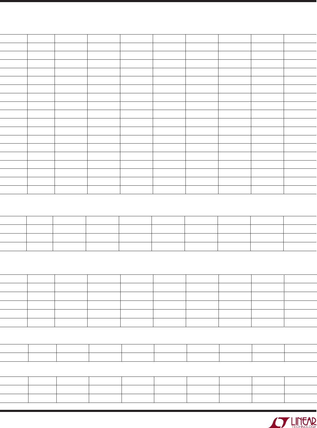
Table 11. Cell Voltage (CV) Register Group
REGISTER RD/WR BIT 7 BIT 6 BIT 5 BIT 4 BIT 3 BIT 2 BIT 1 BIT 0
CVR00 RD C1V[7] C1V[6] C1V[5] C1V[4] C1V[3] C1V[2] C1V[1] C1V[0]
CVR01 RD C2V[3] C2V[2] C2V[1] C2V[0] C1V[11] C1V[10] C1V[9] C1V[8]
CVR02 RD C2V[11] C2V[10] C2V[9] C2V[8] C2V[7] C2V[6] C2V[5] C2V[4]
CVR03 RD C3V[7] C3V[6] C3V[5] C3V[4] C3V[3] C3V[2] C3V[1] C3V[0]
CVR04 RD C4V[3] C4V[2] C4V[1] C4V[0] C3V[11] C3V[10] C3V[9] C3V[8]
CVR05 RD C4V[11] C4V[10] C4V[9] C4V[8] C4V[7] C4V[6] C4V[5] C4V[4]
CVR06 RD C5V[7] C5V[6] C5V[5] C5V[4] C5V[3] C5V[2] C5V[1] C5V[0]
CVR07 RD C6V[3] C6V[2] C6V[1] C6V[0] C5V[11] C5V[10] C5V[9] C5V[8]
CVR08 RD C6V[11] C6V[10] C6V[9] C6V[8] C6V[7] C6V[6] C6V[5] C6V[4]
CVR09 RD C7V[7] C7V[6] C7V[5] C7V[4] C7V[3] C7V[2] C7V[1] C7V[0]
CVR10 RD C8V[3] C8V[2] C8V[1] C8V[0] C7V[11] C7V[10] C7V[9] C7V[8]
CVR11 RD C8V[11] C8V[10] C8V[9] C8V[8] C8V[7] C8V[6] C8V[5] C8V[4]
CVR12 RD C9V[7]
C9V[6] C9V[5] C9V[4] C9V[3] C9V[2] C9V[1] C9V[0]
CVR13 RD C10V[3] C10V[2] C10V[1] C10V[0] C9V[11] C9V[10] C9V[9] C9V[8]
CVR14 RD C10V[11] C10V[10] C10V[9] C10V[8] C10V[7] C10V[6] C10V[5] C10V[4]
CVR15* RD C11V[7] C11V[6] C11V[5] C11V[4] C11V[3] C11V[2] C11V[1] C11V[0]
CVR16* RD C12V[3] C12V[2] C12V[1] C12V[0] C11V[11] C11V[10] C11V[9] C11V[8]
CVR17* RD C12V[11] C12V[10] C12V[9] C12V[8] C12V[7] C12V[6] C12V[5] C12V[4]
*Registers CVR15, CVR16, and CVR17 can only be read if the CELL10 bit in register CFGR0 is low
OPERATION
Table 12. Flag (FLG) Register Group
REGISTER RD/WR BIT 7 BIT 6 BIT 5 BIT 4 BIT 3 BIT 2 BIT 1 BIT 0
FLGR0 RD C4OV C4UV C3OV C3UV C2OV C2UV C1OV C1UV
FLGR1 RD C8OV C8UV C7OV C7UV C6OV C6UV C5OV C5UV
FLGR2 RD C12OV* C12UV* C11OV* C11UV* C10OV C10UV C9OV C9UV
* Bits C11UV, C12UV, C11OV and C12OV are always low if the CELL10 bit in register CFGR0 is high
Table 13. Temperature (TMP) Register Group
REGISTER RD/WR BIT 7 BIT 6 BIT 5 BIT 4 BIT 3 BIT 2 BIT 1 BIT 0
TMPR0 RD ETMP1[7] ETMP1[6] ETMP1[5] ETMP1[4] ETMP1[3] ETMP1[2] ETMP1[1] ETMP1[0]
TMPR1 RD ETMP2[3] ETMP2[2] ETMP2[1] ETMP2[0] ETMP1[11] ETMP1[10] ETMP1[9] ETMP1[8]
TMPR2 RD ETMP2[11] ETMP2[10] ETMP2[9] ETMP2[8] ETMP2[7] ETMP2[6] ETMP2[5] ETMP2[4]
TMPR3 RD ITMP[7] ITMP[6] ITMP[5] ITMP[4] ITMP[3] ITMP[2] ITMP[1] ITMP[0]
TMPR4 RD NA NA NA THSD ITMP[11] ITMP[10] ITMP[9] ITMP[8]
Table 14. Packet Error Code (PEC)
REGISTER RD/WR BIT 7 BIT 6 BIT 5 BIT 4 BIT 3 BIT 2 BIT 1 BIT 0
PEC RD PEC[7] PEC[6] PEC[5] PEC[4] PEC[3] PEC[2] PEC[1] PEC[0]
Table 15. Diagnostic Register Group
REGISTER RD/WR BIT 7 BIT 6 BIT 5 BIT 4 BIT 3 BIT 2 BIT 1 BIT 0
DGNR0 RD REF[7] REF[6] REF[5] REF[4] REF[3] REF[2] REF[1] REF[0]
DGNR1 RD REV[1] REV[0] MUXFAIL NA REF[11] REF[10] REF[9] REF[8]

